YUKAI VSL-BASED Vt-COMPENSATION FOR NAND MEMORY

a vt-based, nand-based technology, applied in static storage, digital storage, instruments, etc., can solve the problems of unintentional errorus reading of nlc data reliability, degrade p/e endurance cycle data reliability, and the vt interfering coupling effect becomes very severe between adjacent bls and wls, so as to achieve less yupin coupling effect, less capacitance, and less capacitan

Active Publication Date: 2016-01-28
LEE PETER WUNG
View PDF5 Cites 59 Cited by
  • Summary
  • Abstract
  • Description
  • Claims
  • Application Information

AI Technical Summary

Benefits of technology

[0142]In a thirty-first embodiment, the present invention discloses a method of performing Odd/Even-BL read operation based on the access WLn status. If the access WLn is a regular non-boundary WL, then a less Yupin coupling effect read can be performed without a VSL-based individual Vt-compensation. Conversely, if the access WLn is a boundary WL like WLn+3, then a severe Yupin coupling effect happens. Thus a VSL-based individual Vt-compensation is preferably performed for a more reliable MLC read. If Yupin coupling effect happens more severe, then the wordline voltage adjustment on the WLn along with individual VSL-based Vt-compensation can be both used for a more reliable MLC read.
[0143]In a thirty-second embodiment, the present invention discloses program-inhibit voltages of Vinh supplied directly from those selected local LBLps power and discharge lines with less capacitance onto those selected LBL lines or CLG, replacing a conventional way from the plurality of long GBL lines of CHG with a heavier parasitic capacitance. As a result, a superior program-inhibit and program with less pow

Problems solved by technology

Unfortunately, a typical NAND array is usually formed in a very compact memory matrix to squeeze die size smaller.
When NAND technology scaling comes to below 30 nm, or even down to 10 nm-class range, the floating-gate Vt interfering coupling effect becomes very severe between adjacent BLs and WLs.
The Yupin coupling effect will result in the nLC data reliability issue of unintentional errorus reading, which is undesired but in fact not avoidable.
However, this is not a perfect BL-shielding method as the BL-BL coupling effect still happens, causing penalties of 2-fold latency of read and program-verify operation, 2-fold Vpass and Vread WL gate disturbance to degrade P/E endurance cycle data reliability of NAND products, and 2-fold power consumption of read, program and verify due to 2 times of half-page size access operations.
On the other hand, although the ABL

Method used


Image

  • YUKAI VSL-BASED Vt-COMPENSATION FOR NAND MEMORY
  • YUKAI VSL-BASED Vt-COMPENSATION FOR NAND MEMORY
  • YUKAI VSL-BASED Vt-COMPENSATION FOR NAND MEMORY

Examples


Embodiment Construction

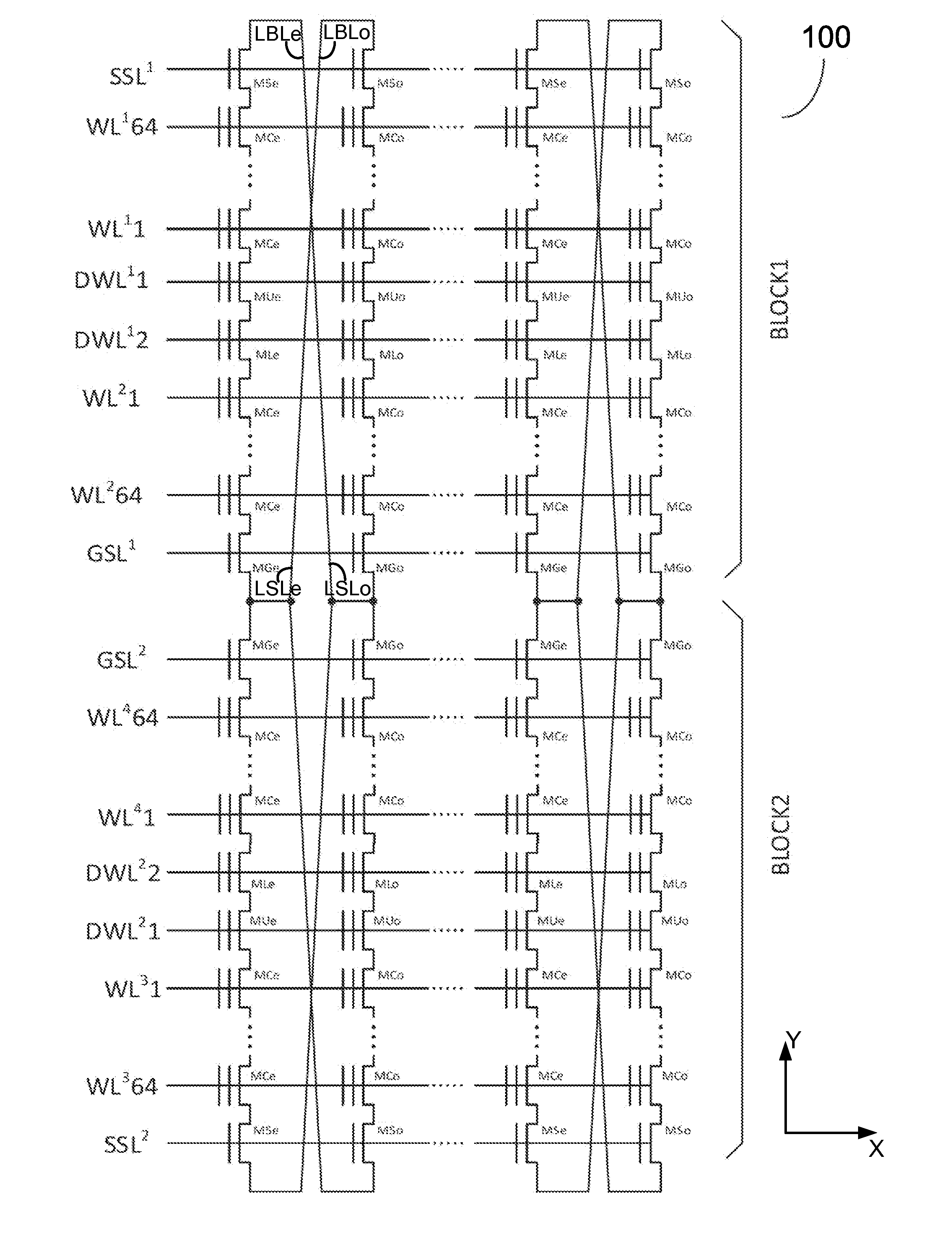
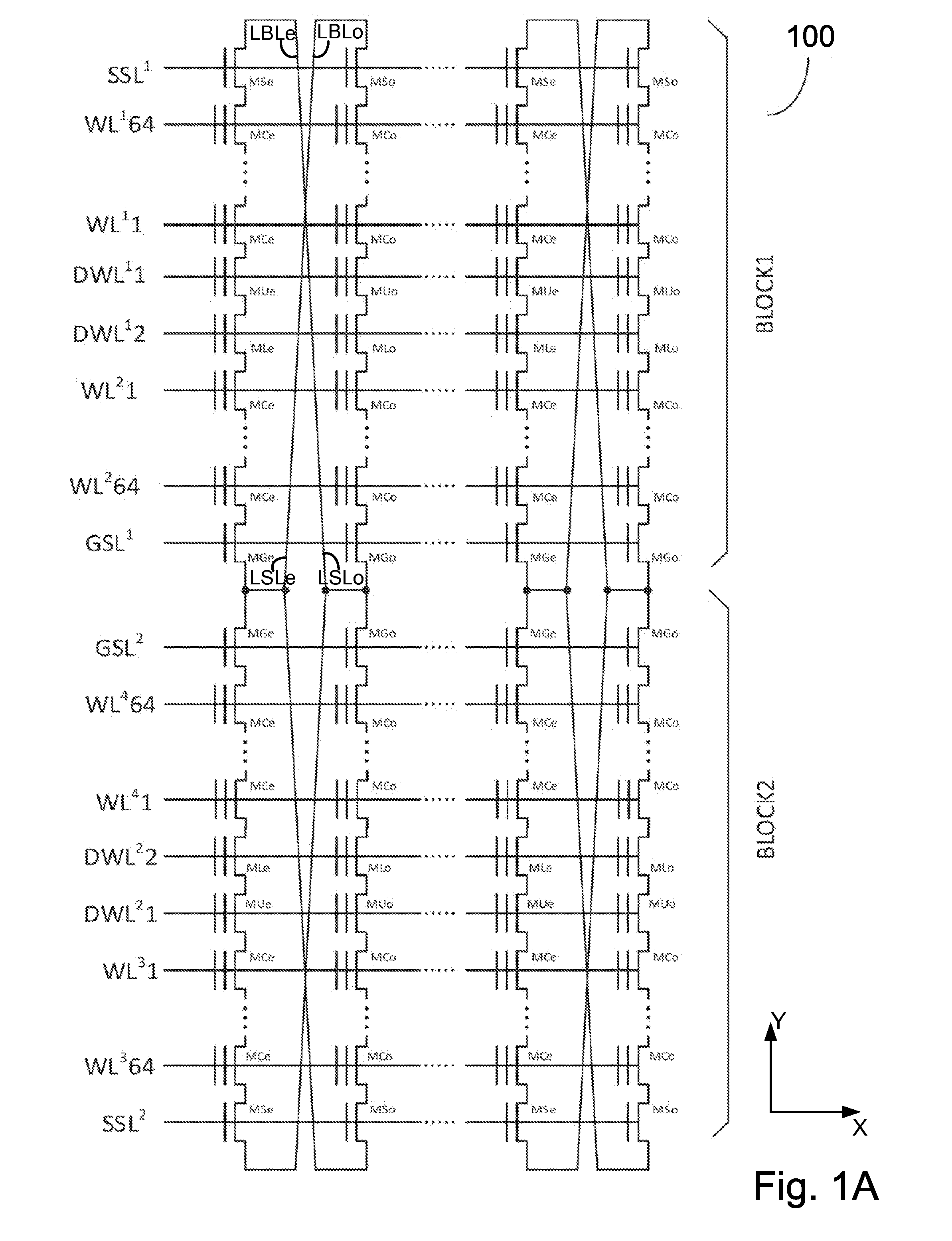
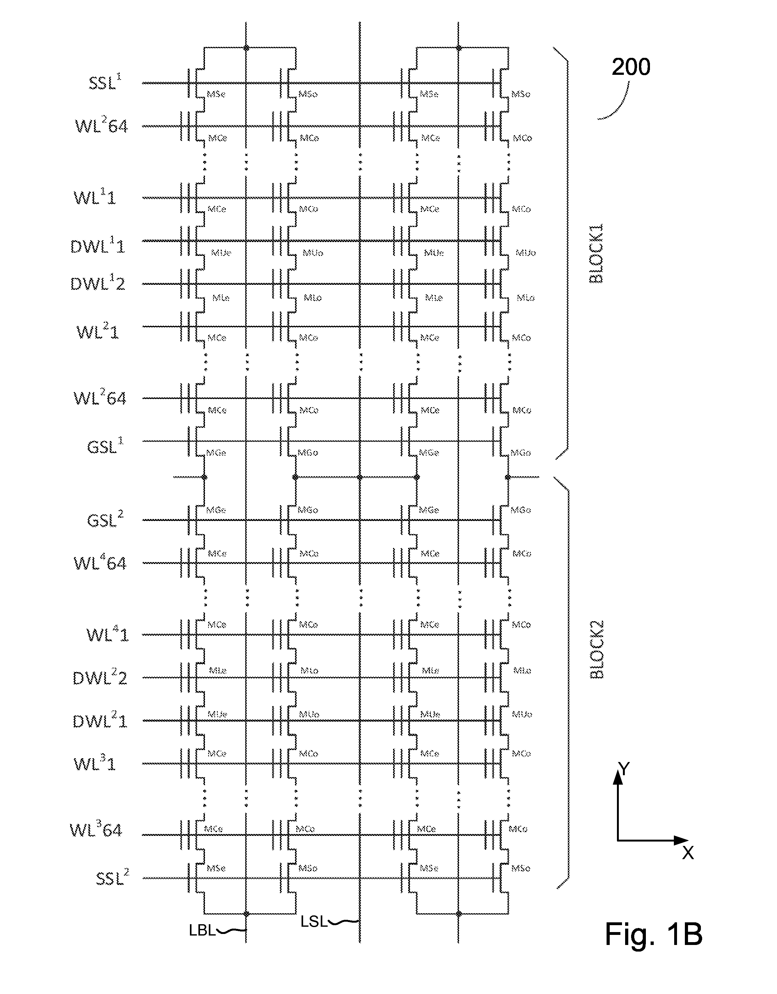
[0238]In the following detailed description of the present embodiments, reference is made to the accompanying drawings that forms a part hereof, and in which is shown, by way of illustration, specific embodiments in which the disclosure may be practiced. In the drawings, like numerals describe substantially similar components throughout the several views. These embodiments are described in sufficient detail to enable those skilled in the art to practice the embodiments. Other embodiments may be utilized and structural, logical, and electrical changes may be made without departing from the scope of the present disclosure. The following detailed description, therefore, not to be taken in a limitation sense.

[0239]As will be known in the subsequent detailed explanation, the goal of the present invention aims to dramatically improve all areas of mainstream nLC NAND designs by at least 10-fold, particularly in 10 nm-class NAND design, regardless of 2D or 3D NAND manufacturing technologies...


PUM


Abstract

A YUKAI NAND array comprising multiple strings associated with hierarchical global/local bit lines (GBL/LBL) and each string being associated with one LBL and having adjacent LBL as a dedicated local source line (LSL) without a common source line to connect all strings. Each of the LBLs is interleavingly associated with either an Odd or Even string selected via one pair of dummy cells inserted in each string and is used as one on-chip PCACHE register with full BL-shielding without wasting extra silicon area to allow batch-based multiple concurrent MLC All-BL, All-Vtn-Program and Alternative-WL program, Odd/Even read and verify operations with options of providing individual and common VSL-based Vt-compensation and VLBL compensations to mitigate high WL-WL and BL-BL coupling effects. Bias conditions in each string are provided to correctly sense highly-negative erase-verify voltage, multiple negative program-verify voltages and without VDS punch-through, breakdown and body-effect in both boundary and non-boundary WLs cells.

Description

1. CROSS-REFERENCES TO RELATED APPLICATIONS[0001]This application claims priority to U.S. Provisional Application No. 62 / 027,694, filed Jul. 22, 2014, commonly assigned and incorporated by reference herein for all purposes.[0002]This application is related to U.S. patent application Ser. No. 14 / 583,178, Ser. No. 14 / 487,078, Ser. No. 14 / 341,739, Ser. No. 14 / 316,936, and Ser. No. 14 / 283,209, incorporated by reference herein for all purposes.[0003]This application is related to following U.S. Pat. Nos. 5,867,429; 6,542,407; 6,522,580; 6,781,877; 6,807,095; 6,847,553; 6,870,768; 6,888,758; 6,917,542; 7,046,548; 7,061,798; 7,102,924; 7,187,585; 7,196,928; 7,196,946; 7,196,928; 7,224,613; 7,289,344; 7,289,348; 7,301,808; 7,301,813; 7,301,839; 7,315,477; 7,321,510; 7,372,730; 7,397,698; 7,443,729; 7,499,329; 7,506,113; 7,522,454; 7,652,929; 7,876,611; 7,876,611; 8,036,041; 8,130,556; 8,274,823; 8,284,606; 8,284,613; 8,400,839; 8,570,810; 8,638,608; 8,705,293; 6,917,542; 7,839,690; 7,499,33...

Claims


Application Information

Patent Timeline
IPC IPC(8): G11C11/56G11C16/04G11C16/08G11C16/14G11C16/24G11C16/26G11C16/34
CPCG11C11/5635G11C11/5642G11C16/14G11C16/26G11C16/08G11C16/0483G11C16/3445G11C16/24G11C16/3459G11C7/14G11C7/18G11C11/56G11C29/50G11C2029/5002
Inventor LEE, PETER, WUNG
Owner LEE PETER WUNG
Why Eureka
Try Eureka