Method for manufacturing semiconductor device

Active Publication Date: 2016-01-28
DENSO CORP
View PDF2 Cites 3 Cited by
  • Summary
  • Abstract
  • Description
  • Claims
  • Application Information

AI Technical Summary

Benefits of technology

The patent text describes a method for manufacturing a semiconductor device that can prevent electric discharge between adjacent semiconductor elements when one of them is being energized. This is achieved by applying a specific potential to a first electrode and using an insulating layer to suppress the occurrence of electric discharge between the first electrode and a nearby second electrode. The technical effect of this method is to improve the manufacturing process for semiconductor devices and prevent issues related to electric discharge, such as damage to the semiconductor elements.

Problems solved by technology

When some semiconductor elements among plural semiconductor elements formed in a semiconductor wafer are energized, electric discharge may occur from an electrode of the semiconductor element being an inspection target to an electrode of an adjacent semiconductor element not being the inspection target, and an occurrence of such a situation is problematic.

Method used


Image

  • Method for manufacturing semiconductor device
  • Method for manufacturing semiconductor device
  • Method for manufacturing semiconductor device

Examples


first embodiment

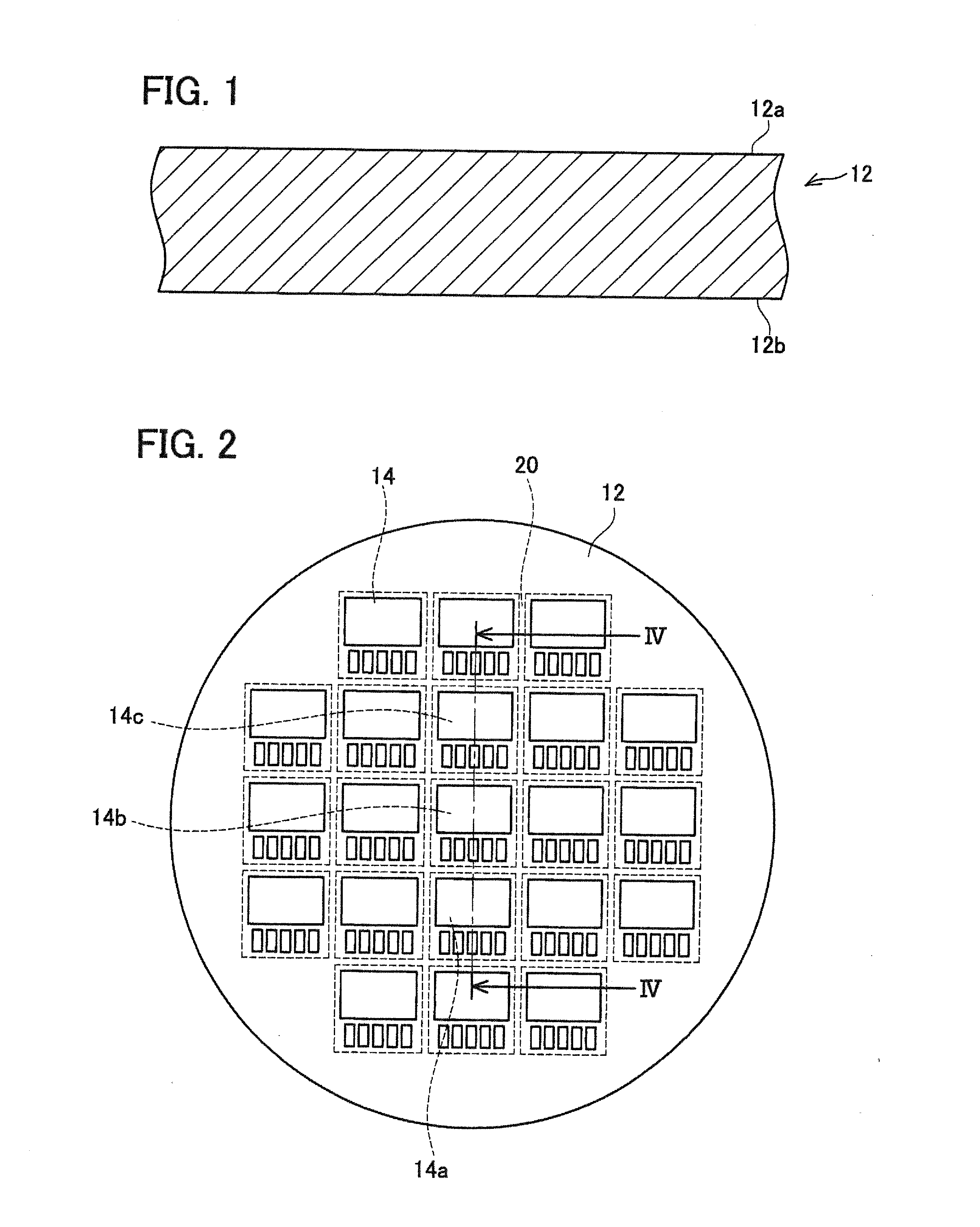
[0030]In a manufacturing method of each of embodiments, a semiconductor device is manufactured from a semiconductor wafer 12 depicted in FIG. 1. For example, an n-type SiC wafer is usable as a semiconductor wafer 12.

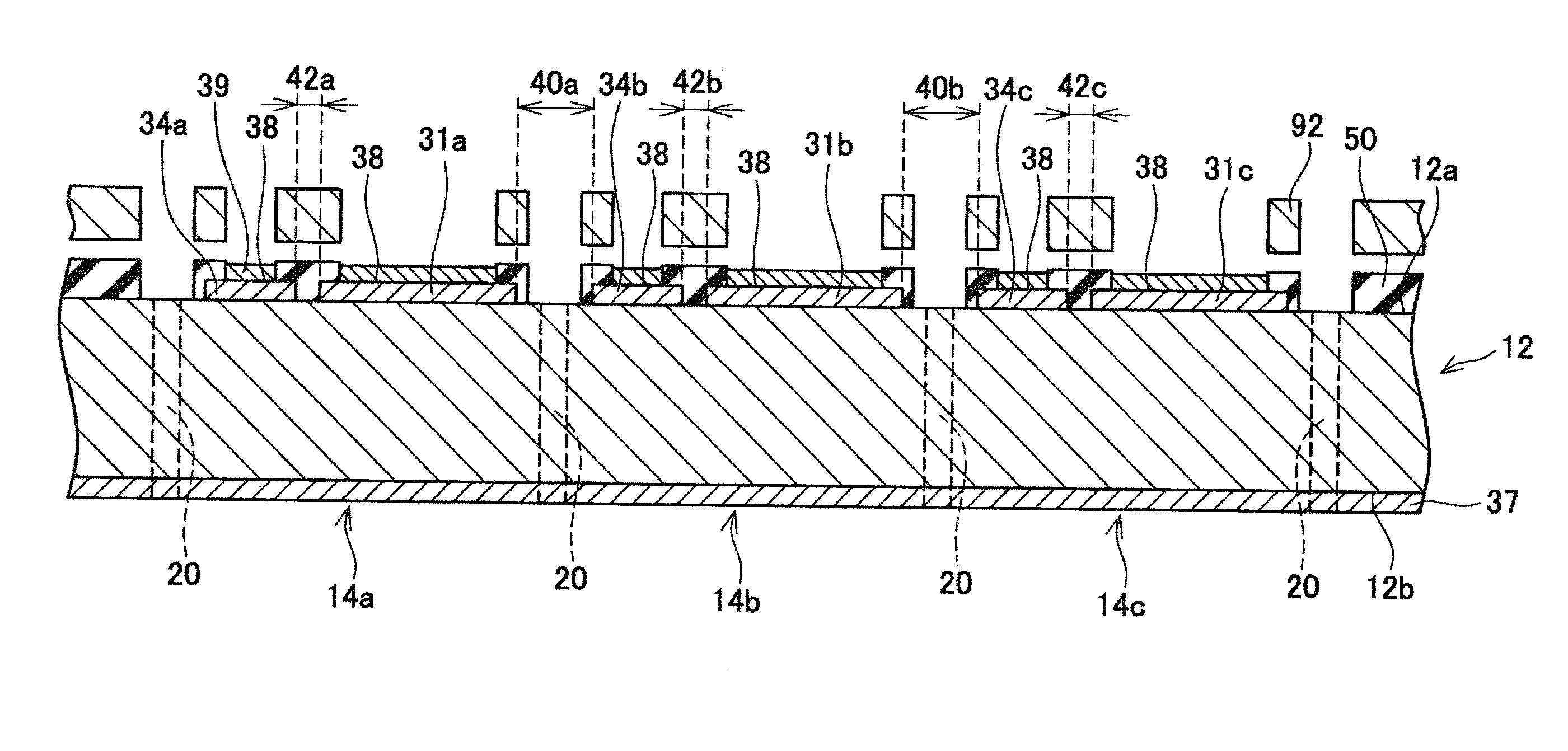
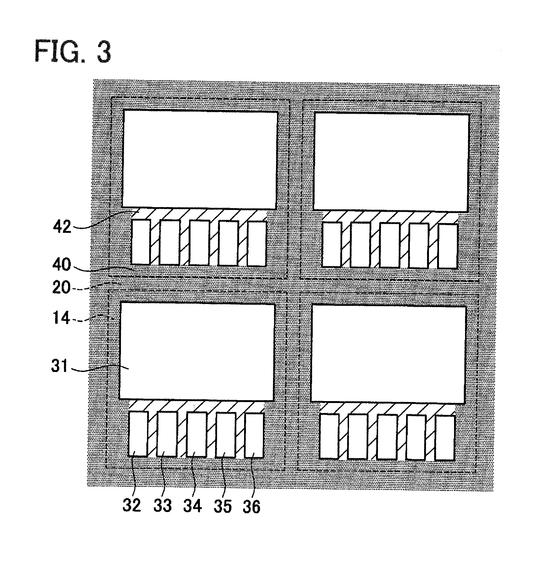
[0031](Semiconductor Element Formation Step) Plural semiconductor elements 14 are formed in the semiconductor wafer 12 as depicted in FIG. 2 by forming p-type diffusion layers, n-type diffusion layers, electrodes, insulating layers, etc., in the semiconductor wafer 12. In FIG. 2, each region surrounded by a dotted line is the semiconductor element 14, and each narrow region located between the adjacent semiconductor elements 14 is a region 20 (that is, a dicing line) to be cut off in a dicing step performed later. In this embodiment, each of the semiconductor elements 14 is an IGBT. As depicted in FIG. 3, each of the semiconductor elements 14 includes electrodes 31 to 36 formed on a top surface 12a of the semiconductor wafer 12. The electrode 31 being the largest electro...

second embodiment

[0042](Semiconductor Element Formation Step) A method of a second embodiment will be described. A semiconductor element formation step of the second embodiment is executed similarly to the semiconductor element formation step of the first embodiment.

[0043](Insulating Layer Formation Step) At an insulating layer formation step, the insulating layer 50 is formed similarly to that of the insulating layer formation step of the first embodiment. As depicted in FIG. 8, however, the insulating layer 50 is formed so that a width of the insulating layer 50 extending from the boundary portion 40 onto the electrode 31 and a width of the insulating layer 50 extending from the boundary portion 40 onto the electrode 34 are wider than those of the first embodiment. More specifically, the insulating layer 50 is formed so that a distance L1 from an edge 31v of the exposed region 38 of the electrode 31 on a boundary portion 40 side to an edge 31w of the electrode 31 on the boundary portion 40 side is...

third embodiment

[0051]A method of a third embodiment will be described. According to the method of the third embodiment, a semiconductor element formation step, an insulating layer formation step, an inspection step, and an insulating layer removal step are executed similarly to those of the second embodiment.

[0052](Metal Film Growth Step) According to the method of the third embodiment, a metal film growth step is executed after the insulating layer removal step is executed. At the metal film growth step, as depicted in FIG. 12, a metal film 39 (in this embodiment, a nickel film) is grown on the surfaces of the exposed regions 38 of the electrodes 31 to 36 by sputtering and employing a same mask as the mask 92 used at the insulating layer removal step. That is, a metal (that is, nickel) sputtering target is placed above the mask 92 and ions of argon, etc., are caused to collide with the sputtering target and, thereby, the metal film 39 is grown. Notably, a state where the mask 92 is fixed to the s...


PUM


Abstract

A method for manufacturing a semiconductor device is provided. The method includes forming a first semiconductor element and a second semiconductor element in a semiconductor wafer. The first semiconductor element includes a first electrode formed on a front surface of the semiconductor wafer. The second semiconductor element is adjacent to the first semiconductor element and includes a second electrode formed on the front surface. The method further includes forming a first insulating layer on the front surface located at a first boundary portion between the first electrode and the second electrode; applying a specific potential different from a potential of the second electrode on the first electrode after the formation of the first insulating layer; and cutting the semiconductor wafer at the first boundary portion so as to divide the first semiconductor element from the second semiconductor element.

Description

CROSS-REFERENCE TO RELATED APPLICATION[0001]This application claims priority to Japanese Patent Application No. 2014-149140 filed on Jul. 22, 2014, the contents of which are hereby incorporated by reference into the present application.TECHNICAL FIELD[0002]A technique disclosed herein relates to a method for manufacturing a semiconductor device.DESCRIPTION OF RELATED ART[0003]Japanese Patent Application Publication No. 2010-177290 discloses a method for inspecting plural semiconductor elements formed on a semiconductor wafer. In this method, the inspection is executed by energizing some semiconductor elements among plural semiconductor elements.BRIEF SUMMARY[0004]When some semiconductor elements among plural semiconductor elements formed in a semiconductor wafer are energized, electric discharge may occur from an electrode of the semiconductor element being an inspection target to an electrode of an adjacent semiconductor element not being the inspection target, and an occurrence of...

Claims


Application Information

Patent Timeline
IPC IPC(8): H01L21/326H01L21/78
CPCH01L21/78H01L21/326H01L21/6835H01L21/6836H01L22/14H01L22/20H01L29/7395
Inventor SOENO, AKITAKAAOI, SACHIKOMIYAHARA, SHINICHIRO
Owner DENSO CORP
Why Eureka
Try Eureka