Rear wide band gap passivated perc solar cells

a solar cell and wide band gap technology, applied in the field of solar cells, can solve the problems of increasing the complexity of the perl cell on an n-type substrate, challenging to achieve high-quality metal recombination shielding, and the solar industry has been extremely conservative in moving to complicated structures, etc., to achieve the effect of reducing the complexity of fabrication, reducing the disadvantages and deficiencies, and improving efficiency

Inactive Publication Date: 2016-02-18
BEAMREACH SOLAR INC
View PDF0 Cites 15 Cited by
  • Summary
  • Abstract
  • Description
  • Claims
  • Application Information

AI Technical Summary

Benefits of technology

[0006]Therefore, a need has arisen for a solar cell structure having improved efficiency and reduced fabrication complexity. In accordance with the disclosed subject matter, rear wide band gap passivated—passivated emitter rear cells are provided which may substantially eliminate or reduce disadvantages and deficiencies associated with previously developed solar cell structures.

Problems solved by technology

Traditionally, the solar industry has been extremely conservative to move to complicated structures because of rigid cost controls.
Providing extra shielding of metal recombination and providing passivation requires additional process steps and high quality metal recombination shielding is challenging to attain.
Making a PERL cell may add more complexity on an n-type substrate as the localized BSF has to be of n++ polarity which cannot necessarily be formed using backside Al metal.
Once again, as previously noted, the trade-off for higher efficiency may be the addition of more process steps and cost.

Method used


Image

  • Rear wide band gap passivated perc solar cells
  • Rear wide band gap passivated perc solar cells
  • Rear wide band gap passivated perc solar cells

Examples


Embodiment Construction

[0013]The following description is not to be taken in a limiting sense, but is made for the purpose of describing the general principles of the present disclosure. The scope of the present disclosure should be determined with reference to the claims. Exemplary embodiments of the present disclosure are illustrated in the drawings, like aspects and identifiers being used to refer to like and corresponding parts of the various drawings.

[0014]And although the present disclosure is described with reference to specific embodiments and components, one skilled in the art could apply the principles discussed herein to other solar cell structures and materials (e.g., mono crystalline silicon or multi-crystalline silicon), fabrication processes (e.g., various deposition methods and materials such as metallization materials), as well as alternative technical areas and / or embodiments without undue experimentation.

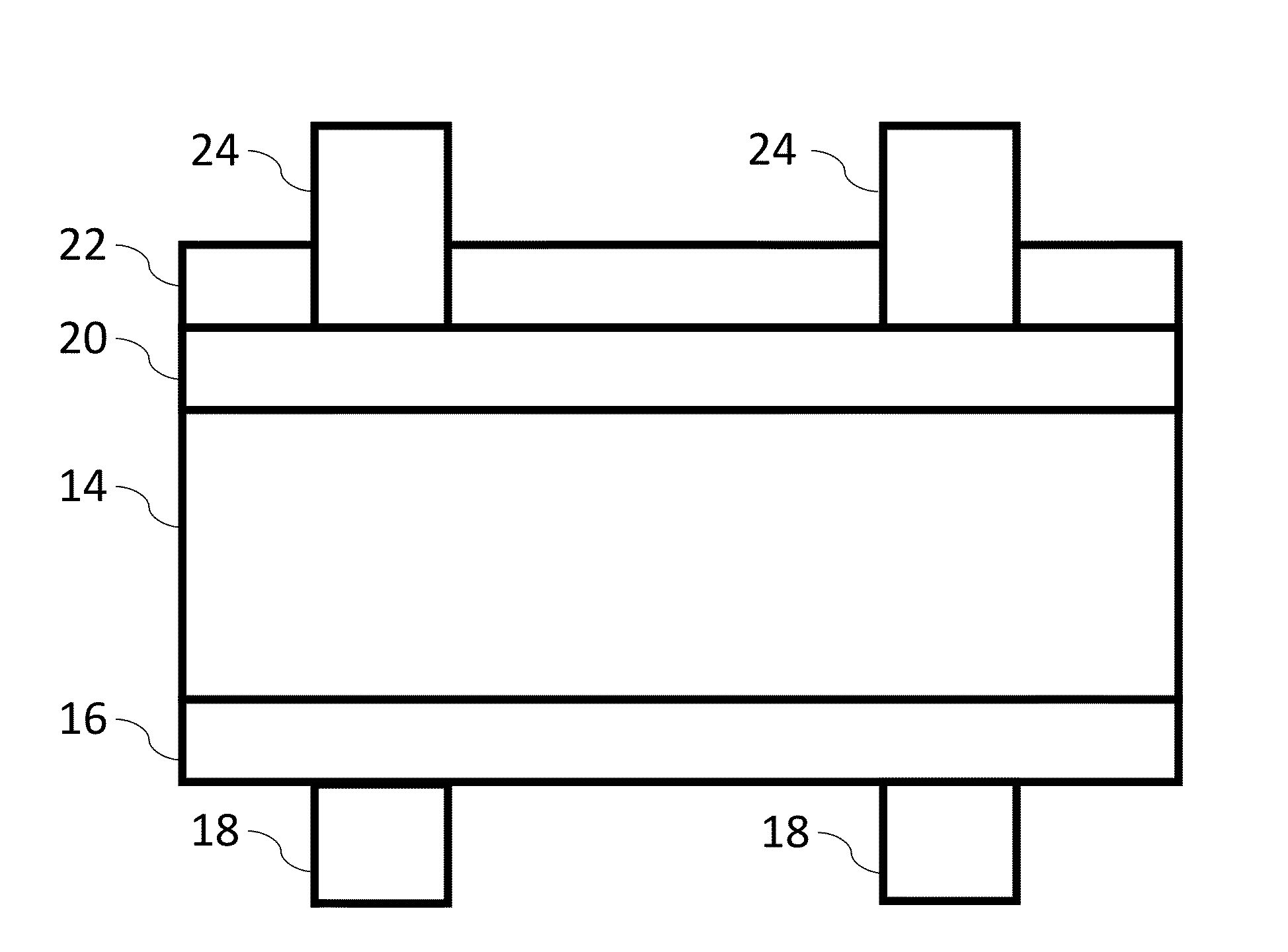
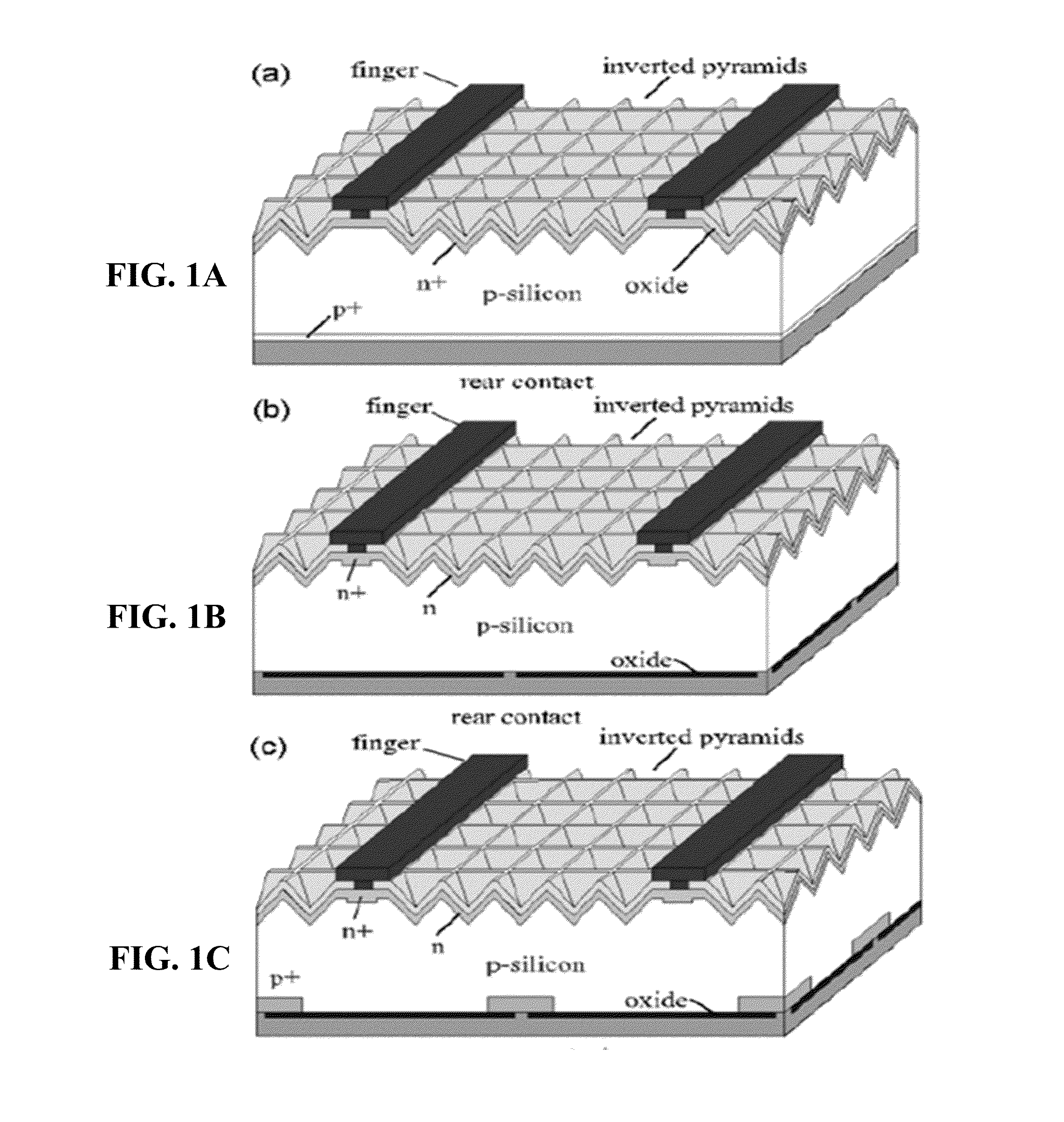
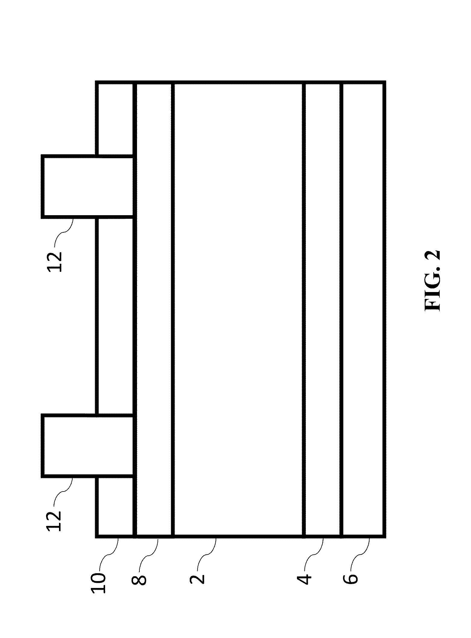
[0015]Rear Wide Band Gap Passivated-Passivated Emitter Rear Cells PERC, referred to...


PUM


Abstract

A photovoltaic solar cell comprises a light absorbing layer of n-type crystalline silicon. An emitter layer is on the front side of the n-type crystalline silicon. A front passivation layer physically contacts the emitter layer. A front metal contact is on the front passivation layer and contacts the emitter layer. A back layer of wide bandgap semiconductor physically contacts a back side of the n-type crystalline silicon layer. A back metal contact physically contacts the wide bandgap semiconductor layer.

Description

CROSS-REFERENCE TO RELATED APPLICATIONS[0001]This application claims the benefit of U.S. provisional patent application 62 / 037,094 filed on Aug. 13, 2014, which is hereby incorporated by reference in its entirety.FIELD OF THE INVENTION[0002]The present disclosure relates in general to the fields of solar cells, and more particularly to wide band gap passivation solar cell structure.BACKGROUND[0003]Passivated emitter solar cells PESC, passivated emitter rear cells PERC, and passivated emitter rear locally diffused PERL solar cells are some of most commonly used cell architectures in the solar industry. FIGS. 1A, 1B, and 1C show schematic diagram for PESC, PERC, and PERL solar cells, respectively. As may be noted in FIGS. 1A, 1B, and 1C, PERL solar cells may be more complicated than PERC and PESC cells; however, more complicated structures may also be capable of providing higher efficiency. Traditionally, the solar industry has been extremely conservative to move to complicated struct...

Claims


Application Information

Patent Timeline
Patent Type & Authority Applications(United States)
IPC IPC(8): H01L31/068H01L31/0216H01L31/0224H01L31/028H01L31/036
CPCH01L31/068H01L31/028H01L31/036H01L31/022441H01L31/02167H01L31/1804Y02E10/547Y02P70/50
Inventor KAPUR, PAWANDESHAZER, HEATHERISLAM, MOHAMMED
Owner BEAMREACH SOLAR INC
Why Eureka
Try Eureka