Signal processing device, optical communication system, and signal processing method

a signal processing and optical communication technology, applied in the field of signal processing devices and signal processing methods, can solve the problems of large non-linear effect received, and the inability to demodulate correct phase information, so as to reduce the size of semiconductor devices without reducing the number of non-linear compensation stages

Active Publication Date: 2016-02-18
NEC CORP
View PDF10 Cites 8 Cited by
  • Summary
  • Abstract
  • Description
  • Claims
  • Application Information

AI Technical Summary

Benefits of technology

[0011]Since filtered back propagation can reduce the number of non-linear compensation stages, it is possible to suppress an increase in the size of the semiconductor device. However, more than a certain number of non-linear compensation stages is required for increasing the accuracy of a signal. The inventors have examined a reduction in the size of the semiconductor device without reducing the number of non-linear compensation stages.
[0012]An object of the present invention is to provide a signal processing device and an optical communication system which are capable of reducing the size of a semiconductor device without reducing the number of non-linear compensation stages.
[0017]According to the present invention, it is possible to reduce the size of a semiconductor device without reducing the number of non-linear compensation stages.

Problems solved by technology

In optical communication of a QAM system, there is a large problem of a non-linear effect which is received when the optical signal propagates through a transmission channel.
Since the QAM system deals with complicated phase information, the reception of phase rotation due to a non-linear effect causes correct phase information not to be capable of being demodulated at the time of reception of the signal.

Method used


Image

  • Signal processing device, optical communication system, and signal processing method
  • Signal processing device, optical communication system, and signal processing method
  • Signal processing device, optical communication system, and signal processing method

Examples


first exemplary embodiment

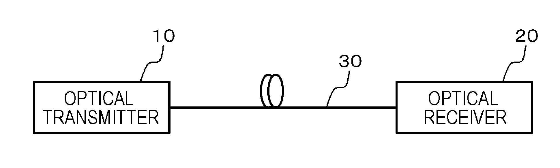
[0029]FIG. 1 is a diagram illustrating a configuration of an optical communication system according to a first exemplary embodiment. The optical communication system according to the present exemplary embodiment includes an optical transmitter 10 and an optical receiver 20. The optical transmitter 10 and the optical receiver 20 are connected to each other through a transmission channel 30. The transmission channel 30 is configured using an optical fiber or the like. This optical communication system is, for example, a system in which communication is performed in a QAM (Quadrature Amplitude Modulation) system.

[0030]The optical transmitter 10 modulates and multiplexes light using a plurality of signals to be transmitted, to thereby generate a polarization-multiplexed optical signal. The generated optical signal is transmitted to the optical receiver 20 through the transmission channel 30. The optical receiver 20 demodulates the received optical signal. The optical signal receives a l...

second exemplary embodiment

[0035]An optical communication system according to the present exemplary embodiment has the same configuration as that of the optical communication system according to the first exemplary embodiment, except for the configuration of an optical receiver 20.

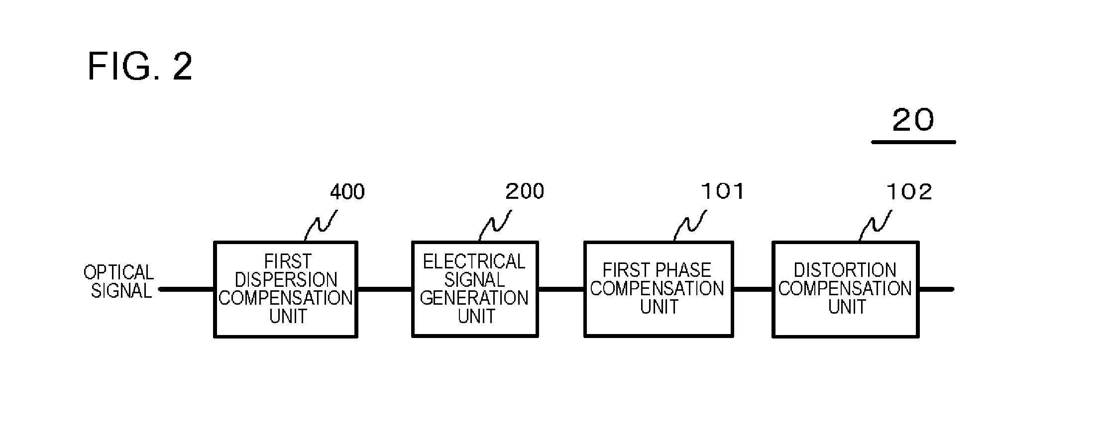
[0036]FIG. 3 is a diagram illustrating a functional configuration of an optical receiver 20 according to the present exemplary embodiment. The optical receiver 20 includes a first dispersion compensation unit 400, a local light source (LO) 210, an optical 90° hybrid 220 (interference unit), a photoelectric (O / E) conversion unit 230, an AD (analog-digital) conversion unit (ADC) 240, and a signal processing unit 100. The signal processing unit 100 is constituted by one semiconductor device.

[0037]As is the case with the first exemplary embodiment, the first dispersion compensation unit 400 performs dispersion compensation on signal light transmitted from the optical transmitter 10, using an optical method.

[0038]The signal light after d...

third exemplary embodiment

[0054]FIG. 7 is a diagram illustrating a functional configuration of an optical transmitter 10 which is used in an optical communication system according to a third exemplary embodiment, and FIG. 8 is a diagram illustrating a functional configuration of an optical receiver 20 according to the present exemplary embodiment. The optical communication system according to the present exemplary embodiment has the same configuration as that of the optical communication system according to the second exemplary embodiment, except that the optical receiver 20 does not include the first dispersion compensation unit 400, and that the optical transmitter 10 instead includes a first dispersion compensation unit 570.

[0055]Specifically, the optical transmitter 10 includes a data generation unit 500, a mapping unit 520, a DA (digital-analog) conversion unit (DAC) 540, an electric-optic conversion (E / O) unit 560, and a first dispersion compensation unit 570. The data generation unit 500 generates a p...


PUM


Abstract

An optical receiver (20) includes an electrical signal generation unit (200), a first phase compensation unit (101), a distortion compensation unit (102), and a first dispersion compensation unit (400). The electrical signal generation unit (200) generates an electrical signal on the basis of received signal light. The first phase compensation unit (101) performs a phase rotation compensation process on the electrical signal generated by the electrical signal generation unit (200). The distortion compensation unit (102) performs a dispersion compensation process and a phase rotation compensation process in this order, at least once, on the electrical signal after having compensation performed thereon by the first phase compensation unit. The electrical signal generation unit (200), the first phase compensation unit (101), and the distortion compensation unit (102) are incorporated into one semiconductor device.

Description

TECHNICAL FIELD[0001]The present invention relates to a signal processing device and a signal processing method which are used in optical communication.BACKGROUND ART[0002]The amount of data communicated has increased with the spread of the Internet. In order to cope with this trend, it is necessary to increase the capacity of a transmission channel. One of techniques for realizing an increase in capacity includes a quadrature amplitude modulation (QAM) system. Optical signals on which modulation of a QAM system is performed in a transmitter are demodulated in an optical receiver of a digital coherent system.[0003]In optical communication of a QAM system, there is a large problem of a non-linear effect which is received when the optical signal propagates through a transmission channel. When the optical signal receives a non-linear effect in the transmission channel, the phase of the optical signal is rotated. Since the QAM system deals with complicated phase information, the recepti...

Claims


Application Information

Patent Timeline
Patent Type & Authority Applications(United States)
IPC IPC(8): H04B10/61H04J14/06
CPCH04B10/6165H04B10/6161H04B10/612H04J14/06H04B10/25133H04B10/613H04B10/614H04B10/6163H04B10/2513
Inventor YASUDA, WAKAKOABE, JUNICHIOGASAHARA, DAISAKU
Owner NEC CORP
Why Eureka
Try Eureka