Manufacturing method of circuit structure embedded with heat-dissipation block

a manufacturing method and heat dissipation block technology, applied in the direction of printed circuit manufacturing, printed circuit aspects, printed element electric connection formation, etc., can solve the problems of increased required manufacturing costs, increased assembly thickness, and increased manufacturing costs, so as to shorten the heat dissipation path of the circuit structure and reduce the assembly thickness of the circuit structure. , the effect of reducing the manufacturing cost of the circuit structur

Active Publication Date: 2016-02-18
UNIMICRON TECH CORP
View PDF27 Cites 26 Cited by
  • Summary
  • Abstract
  • Description
  • Claims
  • Application Information

AI Technical Summary

Benefits of technology

The patent is about a new way to make circuit boards that have a heat-dissipating block. This method reduces the cost of the circuit board while making it thinner and more efficient. This is done by putting the heat-dissipating block in a specific way that reduces the heat-dissipation path and makes it easier to assemble other components. Overall, this method makes it easier to create thin and efficient circuit boards.

Problems solved by technology

Accordingly, a dimension of the heat-dissipation block is greater to cause increases in required manufacturing costs, and a heat-dissipation path of the heat-dissipation block is also longer.
In addition, because the components (e.g., the electronic component, and the heat sink, etc.) are usually directly disposed on an outer surface of the circuit structure and connected to the heat-dissipation block, an assembly thickness may become thicker after aforesaid components are assembled into the circuit structure, which is disadvantageous in miniaturization of the circuit structure.

Method used


Image

  • Manufacturing method of circuit structure embedded with heat-dissipation block
  • Manufacturing method of circuit structure embedded with heat-dissipation block
  • Manufacturing method of circuit structure embedded with heat-dissipation block

Examples


Embodiment Construction

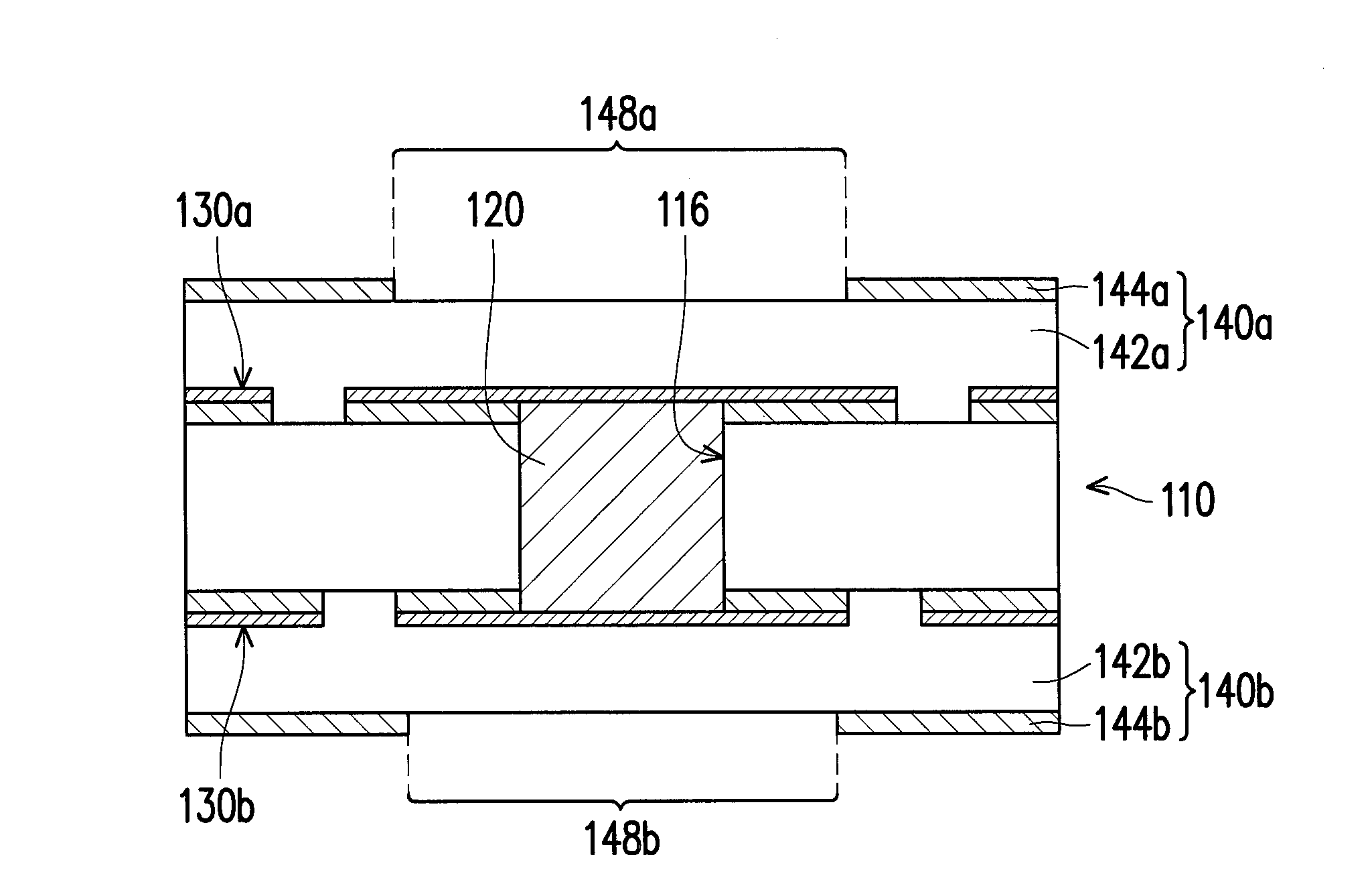
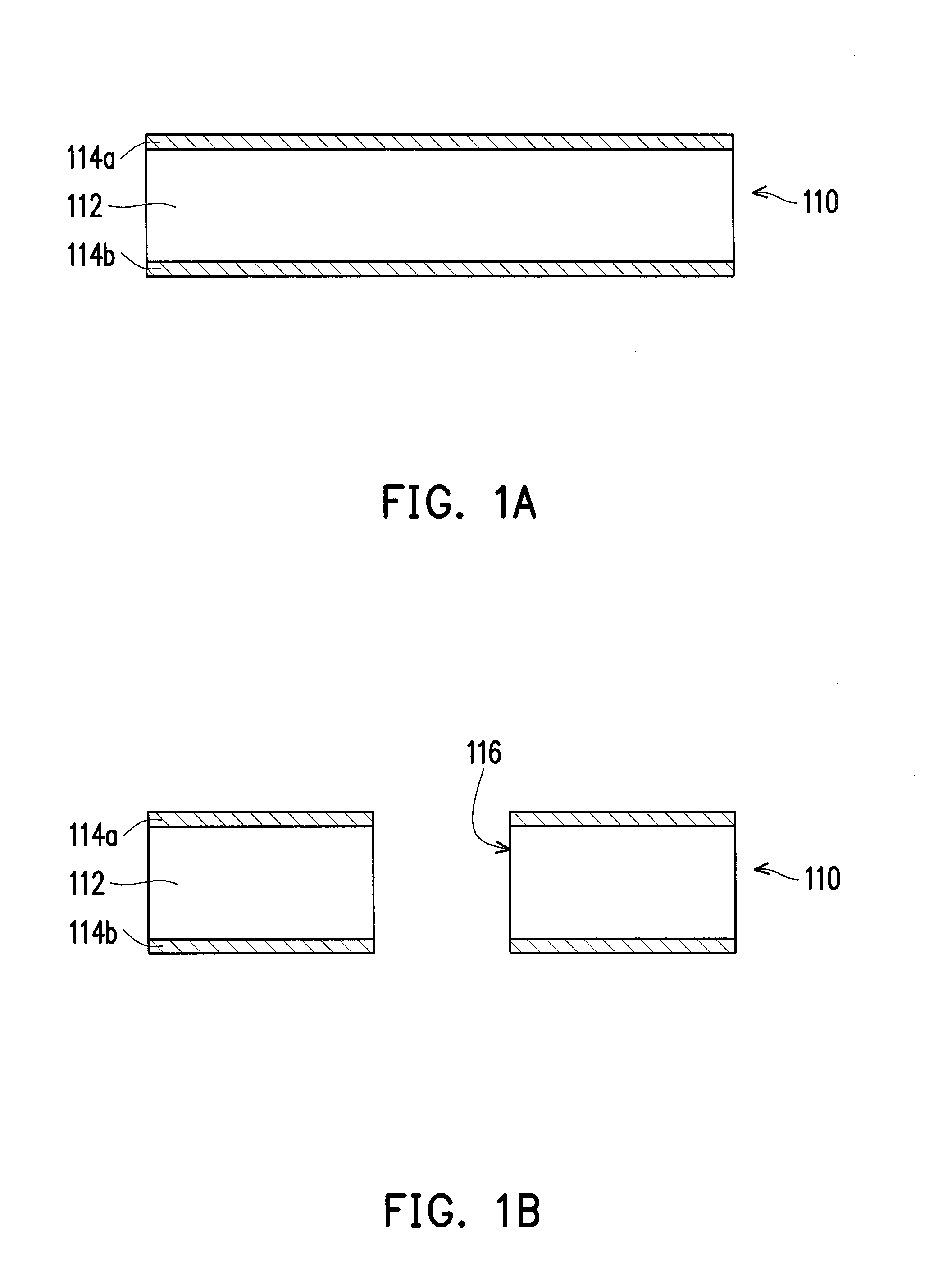
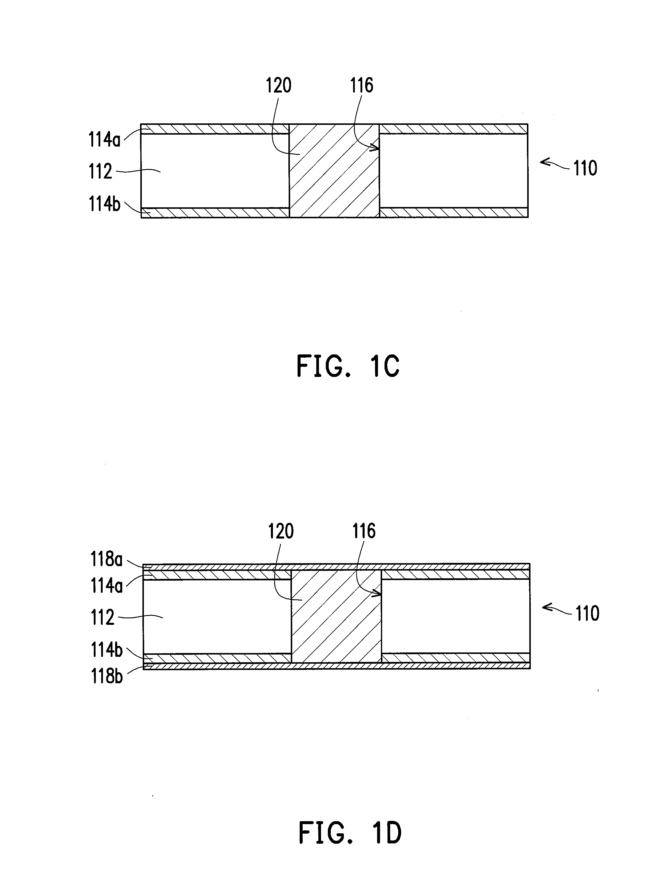
[0018]FIG. 1A to FIG. 1H are schematic diagrams for manufacturing a circuit structure embedded with heat-dissipation block according to an embodiment of the invention. Referring to FIG. 1A to FIG. 1H, in the present embodiment, a manufacturing method of a circuit structure 100 embedded with heat-dissipation block (illustrated in FIG. 1H) includes the following steps. In step S110, a core board 110 is provided. In step S120, a through hole 116 penetrated the core board 110 is formed. In step S130, a heat-dissipation block 120 is disposed into the through hole 116. In step S140, two inner-layer circuits 130a and 130b are formed on two opposite sides of the core board 110. In step S150, build-up structures 140a and 140b are bonded on the core board 110. In step S160, a cavity 146a is formed on a predetermined region 148a of the build-up structure 140a, and a cavity 146b is formed on a predetermined region 148b of the build-up structure 140b, wherein the cavity 146a is communicated with...


PUM


Abstract

A manufacturing method of circuit structure embedded with heat-dissipation block including the following steps is provided. A core board including a first dielectric layer and two first conductive layers located on two opposite sides of the first dielectric layer is provided. A through hole penetrated the core board is formed. A heat-dissipation block is disposed into the through hole. Two inner-layer circuits are formed on two opposite sides of the core board. At least one build-up structure is bonded on the core board, wherein the build-up structure includes a second dielectric layer and a second conductive layer, and the second dielectric layer is located between the second conductive layer and the core board. A cavity is formed on a predetermined region of the build-up structure, and the cavity is communicated with the corresponding inner-layer circuit. Another manufacturing method of circuit structure embedded with heat-dissipation block is also provided.

Description

BACKGROUND OF THE INVENTION[0001]1. Field of the Invention[0002]The invention relates to a manufacturing method of a circuit structure, and more particularly, relates to a manufacturing method of a circuit structure embedded with heat-dissipation block.[0003]2. Description of Related Art[0004]In recent years, for expanding applications of a printed circuit board (PCB), many technologies have been proposed to manufacture the printed circuit board in a multilayer circuit structure in order to increase spaces inside the multilayer circuit structure for circuit layout. A manufacturing method of the multilayer circuit structure includes repeatedly bonding and stacking build-up structures composed of a copper foil and a prepreg (pp) on a core board to increase internal circuit layout spaces in the multilayer circuit structure, and filling conductive materials into blind holes of each of the build-up structures by utilizing an electroplating process in order to conduct through each layer. ...

Claims


Application Information

Patent Timeline
Patent Type & Authority Applications(United States)
IPC IPC(8): H05K1/02H05K3/46H05K3/42
CPCH05K3/4644H05K1/0204H05K3/429H05K1/021H05K1/183H05K3/4602H05K2201/066H05K2201/09845H05K2201/10416
Inventor YU, CHENG-POLI, MING-CHIA
Owner UNIMICRON TECH CORP
Why Eureka
Try Eureka