
NFC card manufacturing

Active Publication Date: 2016-03-03
MOO PRINT
View PDF6 Cites 9 Cited by
  • Summary
  • Abstract
  • Description
  • Claims
  • Application Information

AI Technical Summary

Benefits of technology

The patent describes a method for protecting wireless communication chips during printing and bonding operations by sandwiching them between paper stock and a substrate layer. This is possible without sacrificing the flexibility and manageability of the paper stock. Additionally, the patent describes a method for writing digital information on business cards by sheet-by-sheet, using identifiers such as barcodes or sequential writers to prevent interference and crosstalk between chips. The chips may also have coordinate data representing their position in the sheet to enable simultaneous or sequential writing on multiple sheets.

Problems solved by technology

Despite tools such as Optical Character Recognition, this method is very time consuming and error-prone.
However, 2-D barcodes occupy valuable real-estate on the business card and can spoil the appearance of the business card making this solution less than ideal.
However, the manufacture of existing NFC-enabled business cards is expensive, inflexible and time-consuming.
Furthermore, the incorporation of an NFC chip often detracts from the appearance and quality of high-grade business cards.

Method used


Image

  • NFC card manufacturing
  • NFC card manufacturing
  • NFC card manufacturing

Examples


Embodiment Construction

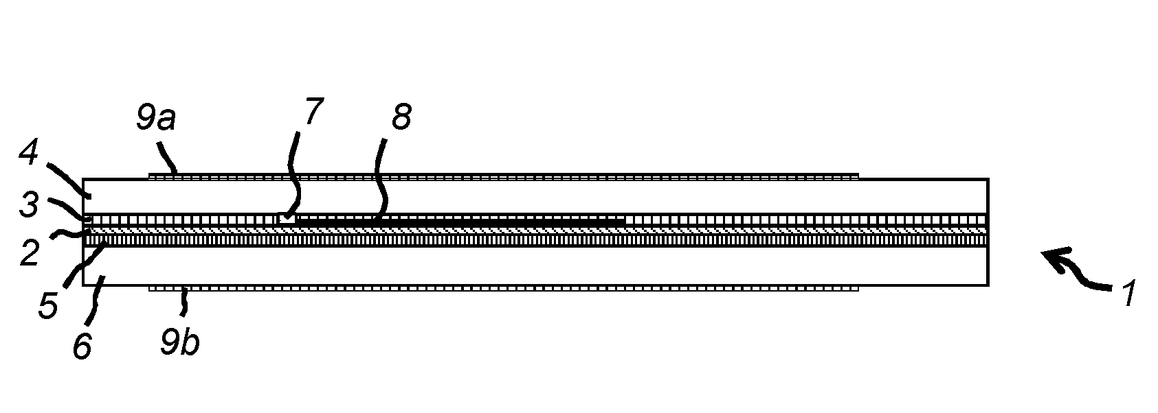
[0064]FIG. 1 shows a cross-sectional schematic view of a multiple ply printed product—in this case, a business card—in accordance with an embodiment of the invention. The multiple ply product 1 comprises a first paper stock 4, a second paper stock 6, a PET substrate layer 2, a wireless communication chip 7 and its corresponding antenna 8. The first and second paper stocks 4, 6 support print 9a, 9b on their respective outwardly-facing surfaces. The first paper stock 4 and the substrate layer 2 are bonded together via a first adhesive layer 3, and the substrate layer 2 and the second paper stock 6 are bonded by a pressure-activated adhesive 5 as will be described in more detail below.

[0065]FIG. 2 shows an exploded view of the product of FIG. 1, with the different plies / layers separated for clarity. In greater detail, the first paper stock 4 comprises: a first outer surface 4a which is able to support print 9a; and a second surface 4b bonded by fluid adhesive 3 to a first surface 2a of...


PUM

PropertyMeasurementUnit
Pressureaaaaaaaaaa
Thicknessaaaaaaaaaa
Pressureaaaaaaaaaa

Abstract

A multiple ply printed product and a method of producing it are described. The method comprises providing a substrate layer having a first surface supporting at least one wireless communication chip and a second surface, reverse to the first surface. A first paper stock having a first surface and a second surface is also provided. A first bonding operation is performed to substantially bond together the first surface of the substrate layer and the second surface of the first paper stock, to sandwich the wireless communication chip between the first paper stock and the substrate layer;providing a second paper stock having a first surface and a second surface. At least one of the first surface of the first paper stock and the second surface of the second paper stock may be printed on. A second bonding operation is performed to bond together the first surface of the second paper stock and the second surface of the substrate layer, to form a multiple ply printed product where the first surface of the substrate layer supports a plurality of wireless communication chips and the multiple ply printed product is a sheet on which is printed a plurality of business cards, each business card corresponding to a respective wireless communication chip.

Description

FIELD OF THE INVENTION[0001]This invention relates to improvements to business cards and specifically to the inclusion of wireless communication chips (for example, NFC chips). In aspects, the invention relates to such business cards and to their manufacture and use.BACKGROUND OF THE INVENTION[0002]Traditionally, business cards have simply included information about the business card holder in printed form. More recently, it has become desirable to ensure that business card information can be easily transferred to the digital domain for use in electronic contact databases and similar electronic systems.[0003]One solution is to scan-in the printed information on the business cards. However, if the digitised information is to be used effectively, such information needs to be interpreted and organised, especially if that information is to be searchable. Despite tools such as Optical Character Recognition, this method is very time consuming and error-prone.[0004]Accordingly, to facilita...

Claims


Application Information

Patent Timeline
IPC IPC(8): B32B37/02B32B37/12B32B38/00G06K19/07
CPCG06K19/07716G06K19/0723B32B37/12B32B38/145B42D15/0093B42D15/02G06K19/07718B32B2425/00B32B2519/02B42D2033/28B42D2033/46B42D25/47B42D25/485B32B2305/342G06K19/07722G06K19/072B32B2317/12B32B37/02B42D25/305
Inventor THOROGOOD, PAUL
Owner MOO PRINT
Learn More