Memory redundancy reduction

a technology of memory redundancy and memory device, applied in the direction of configuration cad, cad techniques, instruments, etc., can solve the problems of data read from the memory to differ from data written, data error rate due to fabrication errors may decrease, etc., to reduce the amount of defective memory locations in the main memory, reduce memory redundancy, and reduce the effect of redundant memory

Inactive Publication Date: 2016-03-03
QUALCOMM INC
View PDF1 Cites 2 Cited by
  • Summary
  • Abstract
  • Description
  • Claims
  • Application Information

AI Technical Summary

Benefits of technology

[0004]Systems and methods to reduce memory redundancy on a memory device are disclosed. A first version of a memory device (e.g., a first chip) may be designed to include main memory and redundant memory. The main memory may include defective memory locations (e.g., storage elements at certain memory addresses) based on fabrication error. Data associated with the defective memory locations may be remapped to memory locations in the redundant memory. As fabrication of the first version of the memory device “matures,” the amount of defective memory locations in the main memory may be reduced. Thus, subsequent versions of the memory device may not need as much redundant memory as the first version of the memory device. When the amount of defective memory locations in the main memory is below a threshold, a second version of the memory device (e.g., a second chip) may be produced that includes less redundant memory than the first version of the memory device. For example, the second version of the memory device may include main memory (e.g., “matured” main memory) that is logically identical to the main memory (with the reduced amount of defective memory locations) of the first version of the memory device. In particular, the main memory of the first version of the memory device and the main memory of the second version of the memory device may be fabricated using an identical fabrication process. Because main memory of the second version of the memory device has a “mature” fabrication data error rate (e.g., a reduced fabrication data error rate), the second version of the memory device may be fabricated with less redundant memory to improve die area. In one aspect, a fixed voltage source may be used (instead of a redundant memory) on the second version of the chip to reduce an amount of die area consumed on the chip.

Problems solved by technology

Data errors may occur at the memory, causing data read from the memory to differ from data written to the memory.
Thus, the memory device may include a quantity of redundant memory.
As the memory device is mass produced, a data error rate due to fabrication errors may decrease over time (e.g., as the fabrication process matures).
Thus, a memory device with an initial fabrication data error rate may utilize more redundant memory than a memory device with a “mature” fabrication data error rate (e.g., a memory device designed according to a mature fabrication process).

Method used


Image

  • Memory redundancy reduction
  • Memory redundancy reduction
  • Memory redundancy reduction

Examples


Embodiment Construction

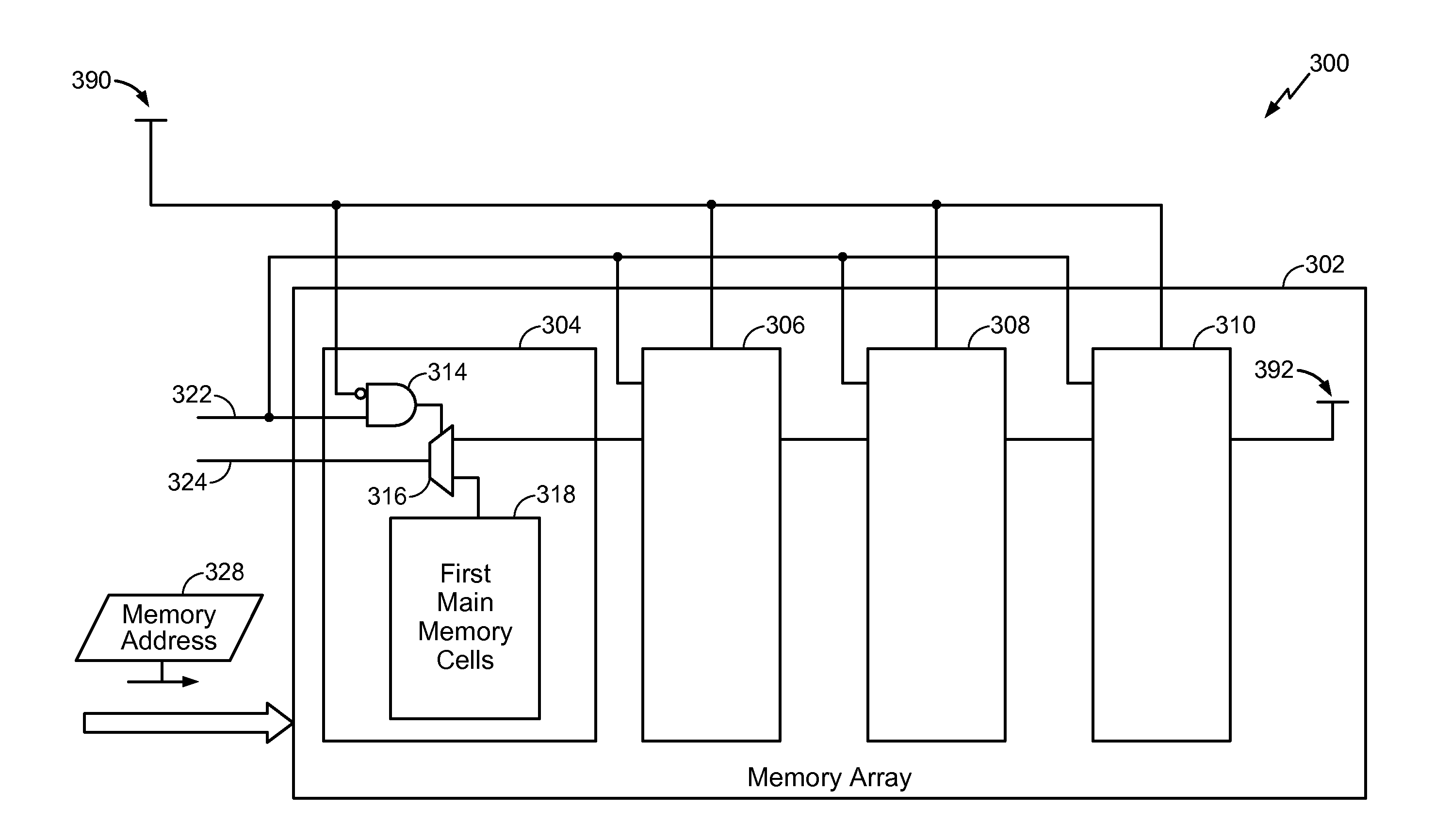
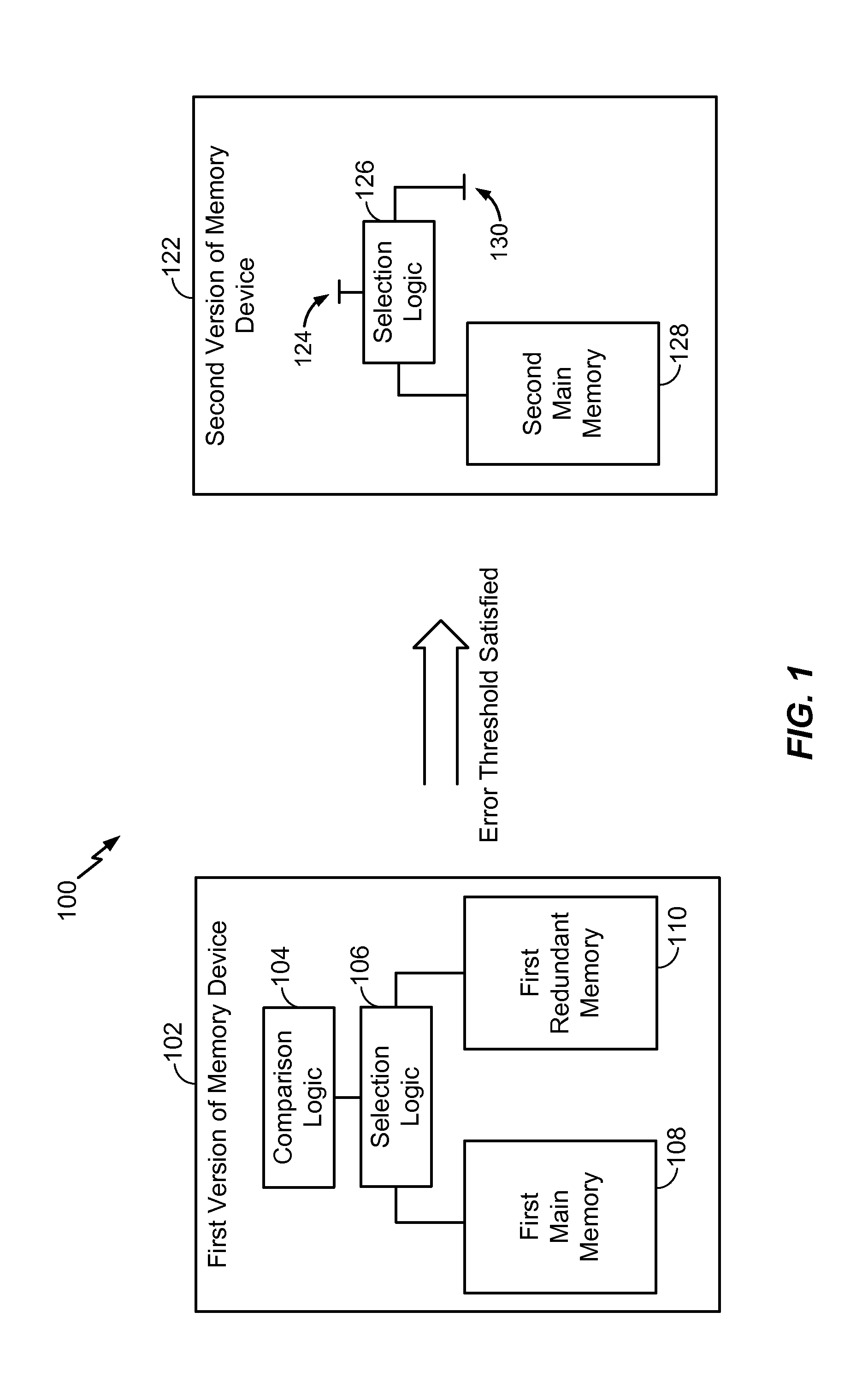
[0018]Referring to FIG. 1, a particular illustrative aspect of a process 100 to reduce an amount of die area occupied by redundant memory on a memory device based on fabrication maturity is shown. The process 100 may be implemented using fabrication techniques and / or fabrication equipment, as described with respect to FIG. 6.

[0019]A first version 102 of a memory device (e.g., a first chip) may be designed at a computer. For example, during a relatively early stage of manufacturing, the computer may generate a first mask to produce the first version 102 of the memory device. The first mask may function as a “blueprint” to manufacture the first version 102 of the memory device on a wafer. For example, the first mask may be used during photolithography (and other wafer fabrication techniques such as wet etching, dry etching, deposition, planarization, etc.) to manufacture components of the first version 102 of the memory device on the wafer.

[0020]The first version 102 of the memory dev...


PUM


Abstract

A method includes designing, at a computer, a first version of a memory device that includes first main memory and first redundant memory. The method further includes modifying a design of the first version of the memory device to produce a second version of the memory device when an error rate associated with fabrication of the first version of the memory device is below a threshold. The second version of the memory device includes second main memory that is logically identical to the first main memory, and the second version of the memory device includes less redundant memory than the first redundant memory.

Description

I. FIELD[0001]The present disclosure is generally related to memory redundancy reduction.II. DESCRIPTION OF RELATED ART[0002]Advances in technology have resulted in smaller and more powerful computing devices. For example, there currently exist a variety of portable personal computing devices, including wireless computing devices, such as portable wireless telephones, personal digital assistants (PDAs), and paging devices that are small, lightweight, and easily carried by users. More specifically, portable wireless telephones, such as cellular telephones and Internet protocol (IP) telephones, can communicate voice and data packets over wireless networks. Further, many such wireless telephones include other types of devices that are incorporated therein. For example, a wireless telephone can also include a digital still camera, a digital video camera, a digital recorder, and an audio file player. Also, such wireless telephones can process executable instructions, including software a...

Claims


Application Information

Patent Timeline
Patent Type & Authority Applications(United States)
IPC IPC(8): G06F17/50
CPCG06F17/5081G06F2217/02G06F2217/06G11C29/54G11C29/72G11C29/76G11C29/80G11C29/814G11C2029/0403G06F30/327G06F2117/02
Inventor LIN, JENTSUNGBASSETT, PAUL, DOUGLAS
Owner QUALCOMM INC
Why Eureka
Try Eureka