Semiconductor device and method for producing semiconductor device

a semiconductor and semiconductor technology, applied in the direction of semiconductor devices, basic electric elements, electrical appliances, etc., can solve the problems of difficult to achieve the reduction of circuit area and difficult to suppress leakage current, and achieve the effect of long deposition time, high integration degree, and double gate length

Active Publication Date: 2016-03-03
UNISANTIS ELECTRONICS SINGAPORE PTE LTD
View PDF7 Cites 1 Cited by
  • Summary
  • Abstract
  • Description
  • Claims
  • Application Information

AI Technical Summary

Benefits of technology

[0017]The present invention can provide a semiconductor device having a high integration degree.
[0018]As described above, a semiconductor device includes a first pillar-shaped semiconductor layer formed on a semiconductor substrate; a first first-conductivity-type semiconductor layer formed in the first pillar-shaped semiconductor layer; a third first-conductivity-type semiconductor layer formed in the first pillar-shaped semiconductor layer and located at a higher position than the first first-conductivity-type semiconductor layer; a first gate insulating film formed so as to surround a region of the first pillar-shaped semiconductor layer, the region being sandwiched between the first first-conductivity-type semiconductor layer and the third first-conductivity-type semiconductor layer; a first gate formed so as to surround the first gate insulating film; a second gate insulating film formed so as to surround a region of the first pillar-shaped semiconductor layer, the region being sandwiched between the first first-conductivity-type semiconductor layer and the third first-conductivity-type semiconductor layer; and a second gate formed so as to surround the second gate insulating film, wherein the first gate and the second gate are mutually connected. This configuration can provide a semiconductor device in which the gate length is doubled. In general, in order to provide a gate having a large gate length, metal needs to be deposited to a large thickness by atomic layer deposition to fill a recess region having a height corresponding to the gate length; atomic layer deposition of depositing atom layer by atom layer to a large thickness requires long deposition time, which results in an increased production time. In contrast, according to the present invention, the recess regions for gates can be designed so as to have relatively low heights. Thus, deposition of metal to a small thickness by atomic layer deposition will suffice, and the deposition time for atomic layer deposition can be shortened, which results in a decreased production time.

Problems solved by technology

As reduction in the size of MOS transistors proceeds, leakage current is difficult to suppress.
Accordingly, from the standpoint of providing a necessary current, reduction in circuit area is difficult to achieve, which has been problematic.

Method used


Image

  • Semiconductor device and method for producing semiconductor device
  • Semiconductor device and method for producing semiconductor device
  • Semiconductor device and method for producing semiconductor device

Examples


Embodiment Construction

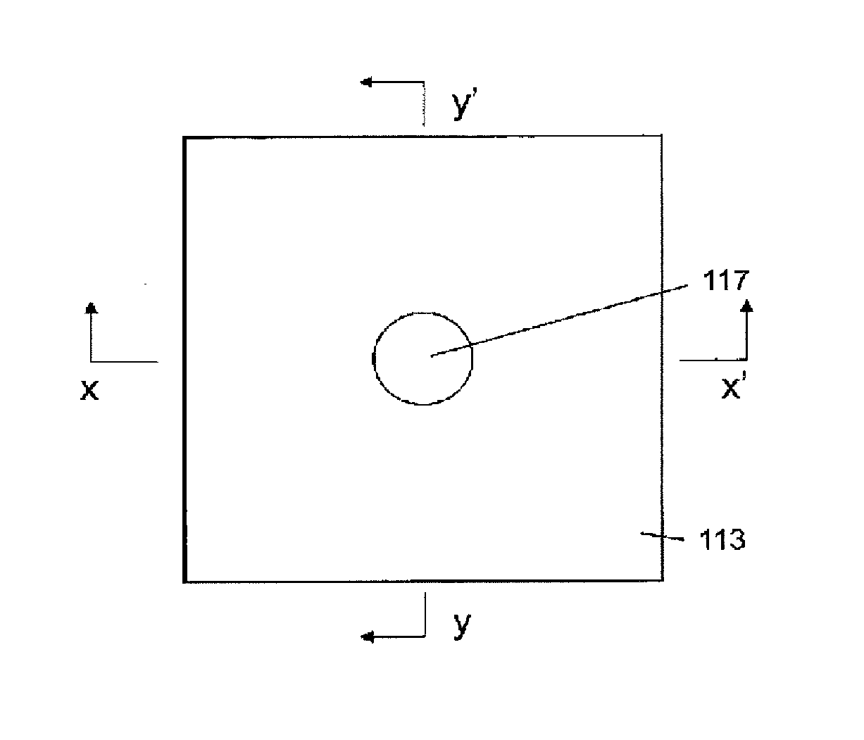
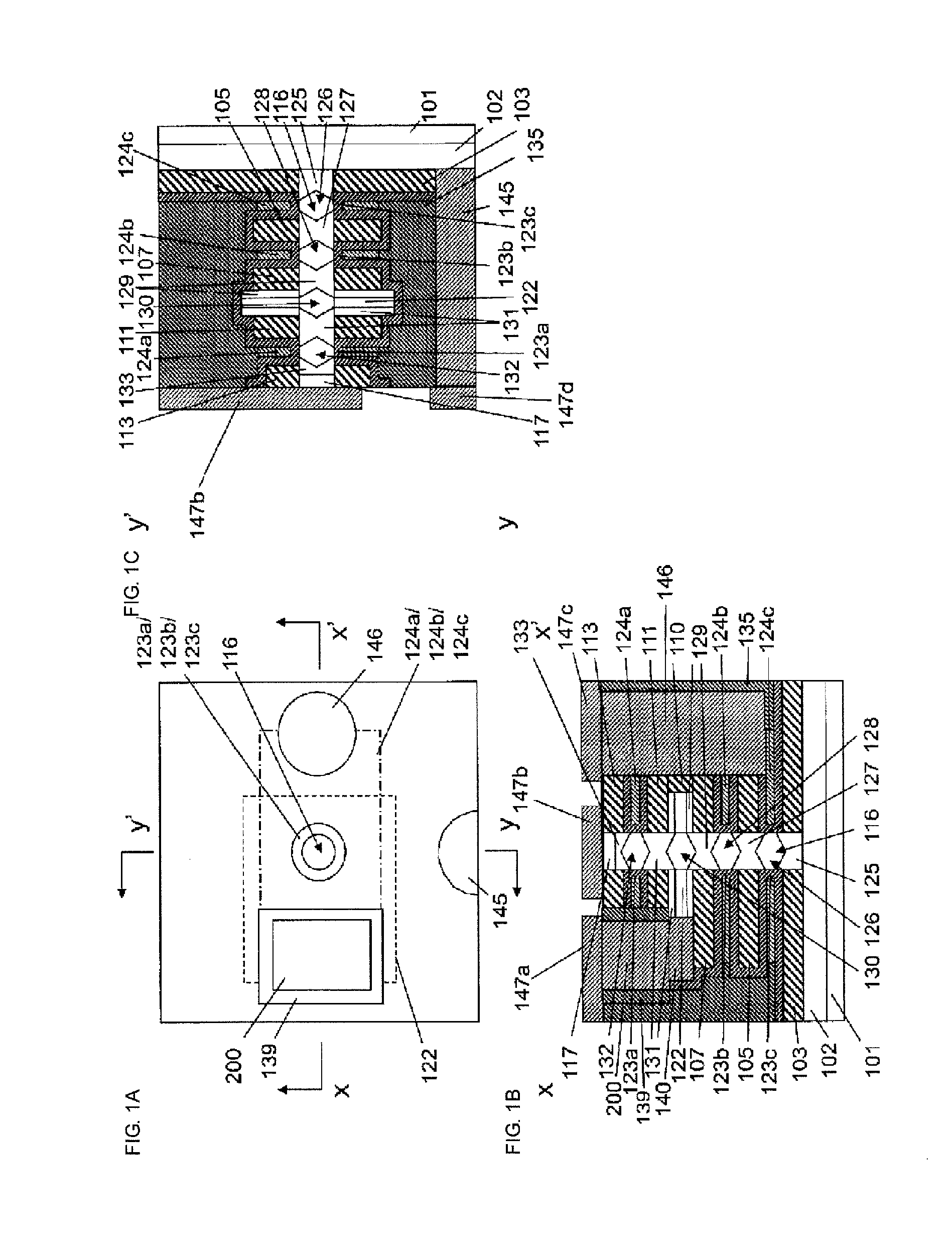
[0143]Hereinafter, an embodiment according to the present invention will be described. FIGS. 1A to 1C illustrate the structure of a semiconductor device according to an embodiment of the present invention. In this embodiment, silicon is used as the semiconductor. Alternatively, a semiconductor other than silicon may be used.

[0144]The semiconductor device includes a first pillar-shaped silicon layer 116 formed on a silicon substrate 101; a first first-conductivity-type silicon layer 125 formed in the first pillar-shaped silicon layer 116; a third first-conductivity-type silicon layer 129 formed in the first pillar-shaped silicon layer 116 and located at a higher position than the first first-conductivity-type silicon layer 125; a first gate insulating film 123c formed so as to surround a region of the first pillar-shaped silicon layer 116, the region being sandwiched between the first first-conductivity-type silicon layer 125 and the third first-conductivity-type silicon layer 129; a...


PUM

PropertyMeasurementUnit
conductivityaaaaaaaaaa
conductivity typeaaaaaaaaaa
insulatingaaaaaaaaaa

Abstract

A semiconductor device includes a first pillar-shaped semiconductor layer formed on a semiconductor substrate; a first first-conductivity-type semiconductor layer formed in the first pillar-shaped semiconductor layer; a third first-conductivity-type semiconductor layer formed in the first pillar-shaped semiconductor layer and located at a higher position than the first first-conductivity-type semiconductor layer; a first gate insulating film formed so as to surround a region of the first pillar-shaped semiconductor layer sandwiched between the first first-conductivity-type semiconductor layer and the third first-conductivity-type semiconductor layer; a first gate formed so as to surround the first gate insulating film; a second gate insulating film formed so as to surround a region of the first pillar-shaped semiconductor layer sandwiched between the first first-conductivity-type semiconductor layer and the third first-conductivity-type semiconductor layer; and a second gate formed so as to surround the second gate insulating film, wherein the first gate and the second gate are mutually connected.

Description

CROSS REFERENCES TO RELATED APPLICATION[0001]The present application claims priority to PCT / JP2014 / 072563, filed Aug. 28, 2014. The contents of the application are incorporated herein by reference in their entirety.BACKGROUND OF THE INVENTION[0002]1. Field of the Invention[0003]The present invention relates to a semiconductor device and a method for producing a semiconductor device.[0004]2. Description of the Related Art[0005]In semiconductor integrated circuits, in particular, integrated circuits including MOS transistors, the integration degree has been continuously increased. With this increase in the integration degree, the size of MOS transistors used in integrated circuits has been reduced to the order of nanometers. As reduction in the size of MOS transistors proceeds, leakage current is difficult to suppress. Accordingly, from the standpoint of providing a necessary current, reduction in circuit area is difficult to achieve, which has been problematic. In order to address su...

Claims


Application Information

Patent Timeline
Patent Type & Authority Applications(United States)
IPC IPC(8): H01L29/51H01L21/768H01L27/02H01L27/115H01L29/423
CPCH01L29/511H01L27/115H01L21/76883H01L29/42392H01L21/76805H01L27/0207H01L29/66666H01L29/7827H01L21/76897
Inventor MASUOKA, FUJIONAKAMURA, HIROKI
Owner UNISANTIS ELECTRONICS SINGAPORE PTE LTD
Why Eureka
Try Eureka