Production method for organic electroluminescent element
- Summary
- Abstract
- Description
- Claims
- Application Information
AI Technical Summary
Benefits of technology
Problems solved by technology
Method used
Image
Examples
example 1
[0175]
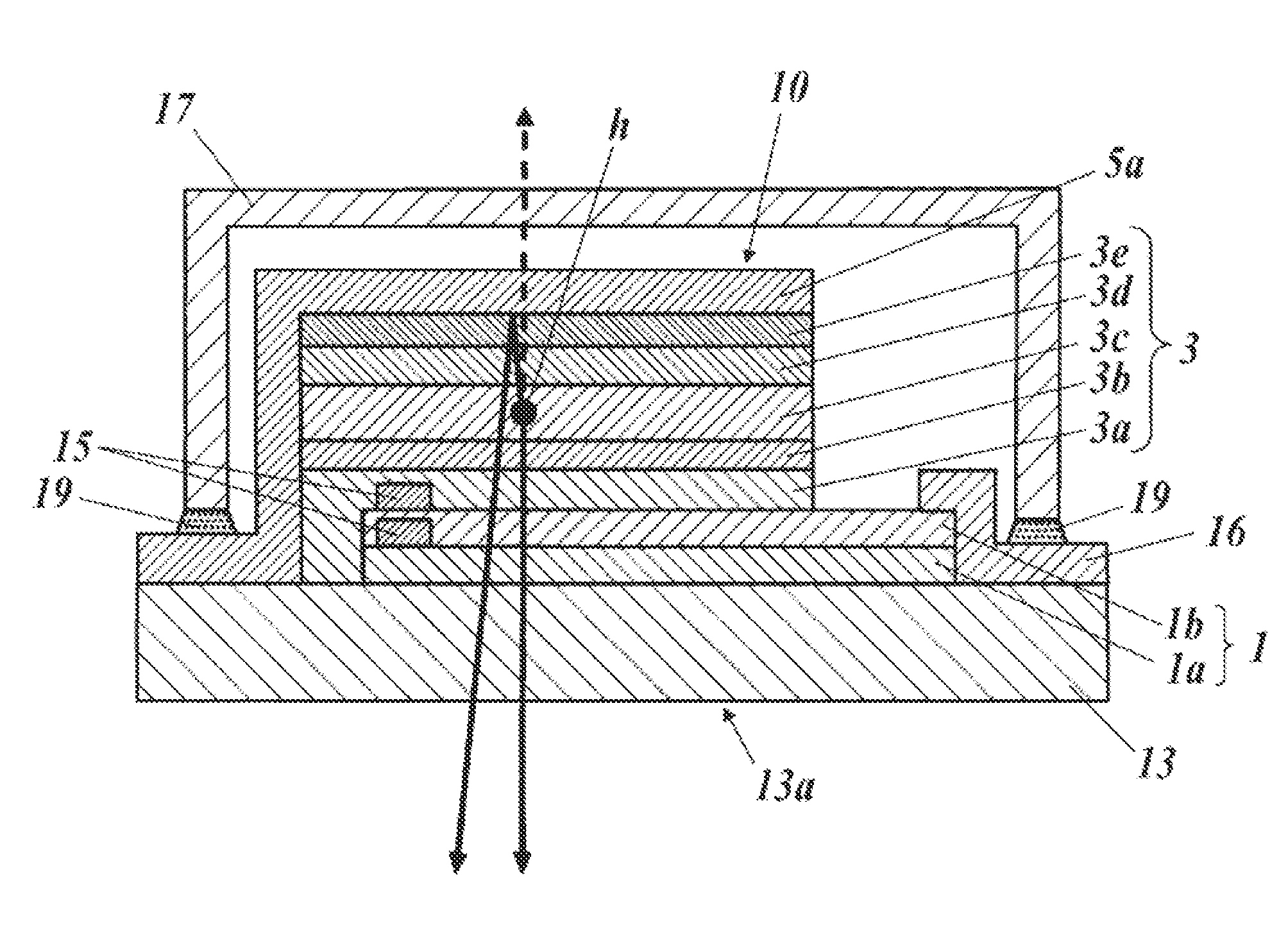
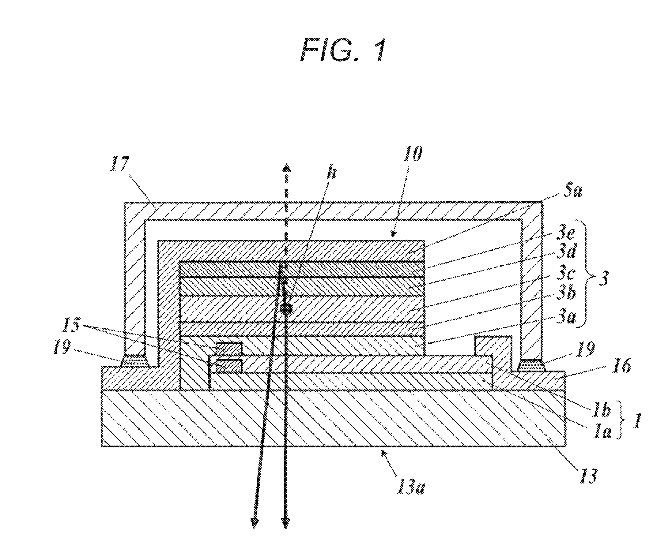
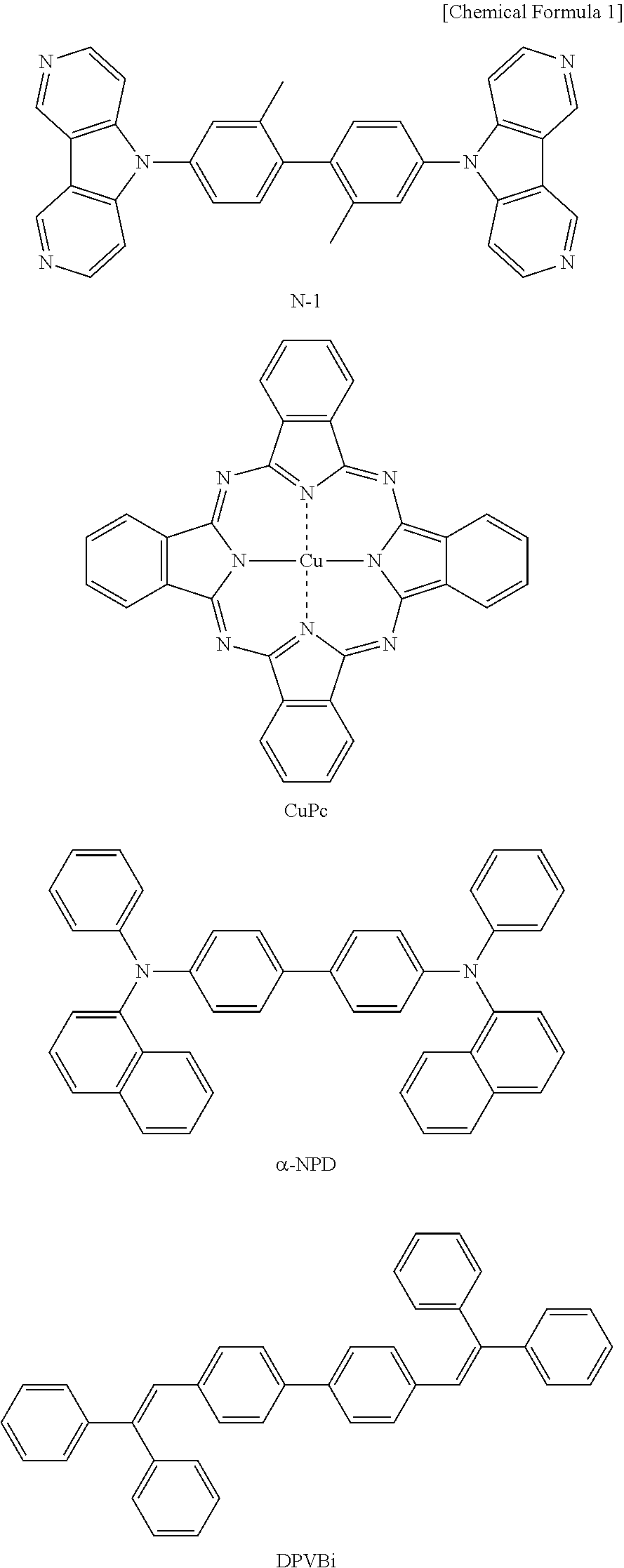
[0176]Nitrogen-containing compound N-1 represented by the following formula was formed into a film at a thickness of 25 nm on a PET transparent resin substrate having a thickness of 75 μm and having a gas barrier layer in which polysilazane and an organic layer (stress relaxation layer) have been stacked, and silver was formed into a film at a thickness of 10 nm as an anode by using a mask in a vacuum deposition apparatus. The gas barrier layer of the transparent resin substrate was formed in a similar manner to that for the barrier film sample 1 in Example 1 of JP 2012-599 A.
[0177]Furthermore, CuPc (copper phthalocyanine) as a hole injection material, α-NPD as a hole transport material, DPVBi as a host compound for a blue light emitting layer, FIr(pic) as a dopant for the blue light emitting layer, CBP as a host compound for a green light emitting layer, Ir(ppy)3 as a dopant for the green light emitting layer, Ir(piq)3 as a dopant for a red light emitting layer, BAlq as a hol...
example 2
[0217]
[0218]An organic EL element 201 was prepared in a similar manner, except that the resin substrate was changed from PET to PEN and the ultraviolet ray irradiation time was set to 6 hours in the preparation of the organic EL element 101.
[0219]
[0220]Organic EL elements 202 to 205 were prepared in a similar manner, except that the cut wavelength (transmittance 50%) of the ultraviolet absorption filter was changed to 340 nm, 350 nm, 370 nm and 380 nm, respectively, as shown in Table 2, in the preparation of organic EL element 201.
[0221]
[0222]An organic EL element 206 was prepared in a similar manner, except that irradiation with ultraviolet ray was conducted without using an ultraviolet absorption filter in the preparation of the organic EL element 201.
[0223]
[0224]An organic EL element 207 was prepared in a similar manner, except that the resin substrate was changed from PEN to PC in the preparation of the organic EL element 201.
[0225]
[0226]Organic EL elements 208 to 211 were prepa...
example 3
[0239]
[0240]Nitrogen-containing compound N-1 was formed into a film at a thickness of 25 nm on a PET transparent resin substrate having a gas barrier layer on which polysilazane and an organic layer (stress relaxation layer) had been stacked and having a thickness of 125 μm in a vacuum deposition apparatus, and silver was formed into a film as an anode at a thickness of 10 nm by using a mask.
[0241]A hole injection layer, a hole transport layer, a blue light emitting layer, a first medium layer, a green light emitting layer, a second medium layer and a red light emitting layer were disposed on this resin substrate in a similar manner to the preparation of the organic EL element 101.
[0242]Furthermore, nitrogen-containing compound N-1 was deposited to form a film at a thickness of 20 nm on a red light emitting layer, and silver was deposited thereon to dispose a cathode having a layer thickness of 10 nm.
[0243]Furthermore, the side of the above-mentioned deposited surface was covered wi...
PUM
 Abstract
Description
Claims
Application Information


