Group iii nitride semiconductor light-emitting device and production method therefor

a technology of nitride semiconductors and light-emitting devices, which is applied in the direction of semiconductor/solid-state device manufacturing, semiconductor devices, electrical equipment, etc., can solve the problems of short lifetime of light-emitting devices, inability to suppress the migration of ag atoms or al atoms, etc., and achieve the effect of simplifying the production method

Active Publication Date: 2016-03-17
TOYODA GOSEI CO LTD
View PDF6 Cites 5 Cited by
  • Summary
  • Abstract
  • Description
  • Claims
  • Application Information

AI Technical Summary

Benefits of technology

[0033]The present specification provides a Group III nitride semiconductor light-emitting device in which the production...

Problems solved by technology

However, a light-emitting device in which migration of ...

Method used


Image

  • Group iii nitride semiconductor light-emitting device and production method therefor
  • Group iii nitride semiconductor light-emitting device and production method therefor
  • Group iii nitride semiconductor light-emitting device and production method therefor

Examples


example 1

3-2-1. Example 1

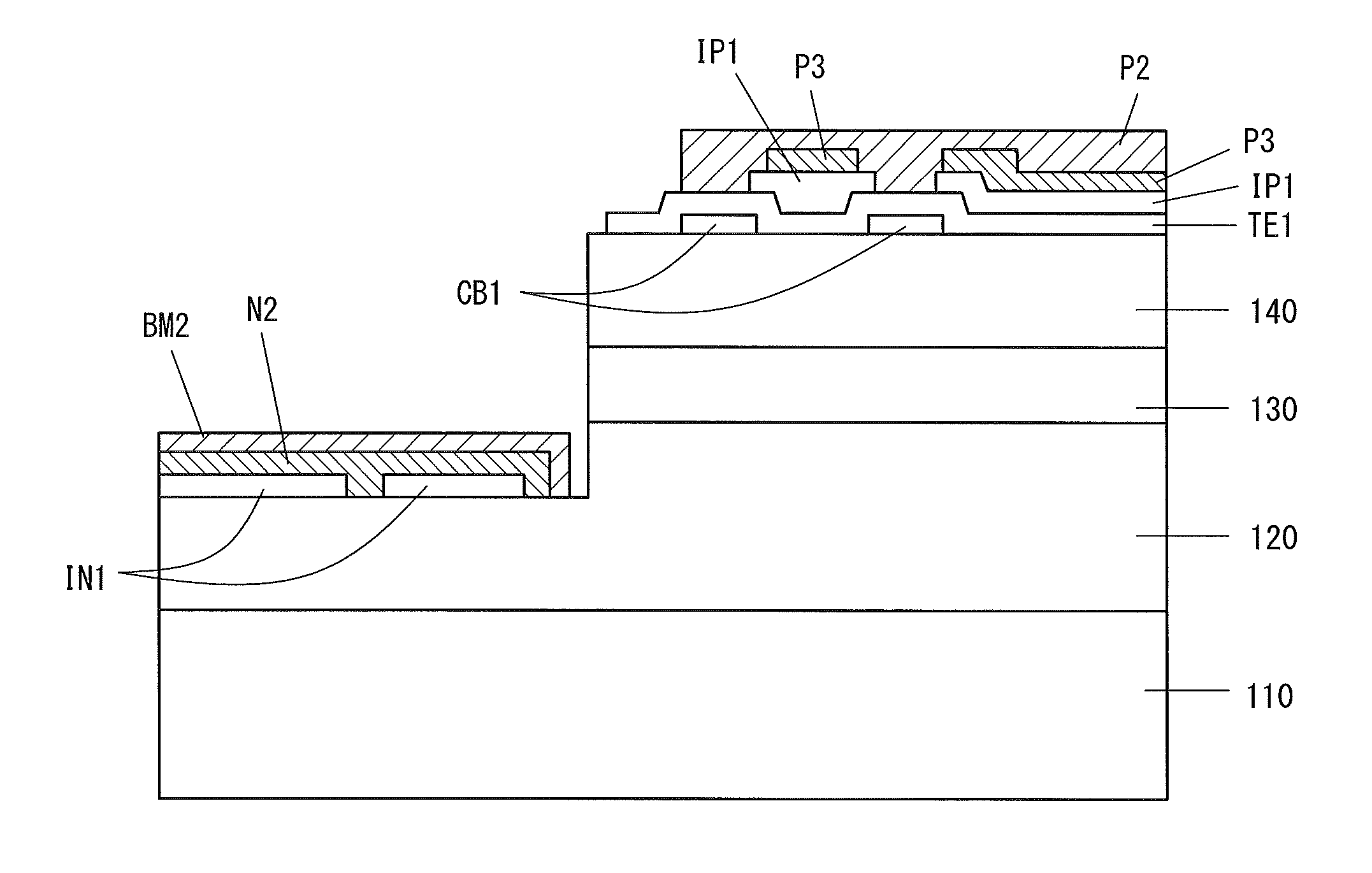
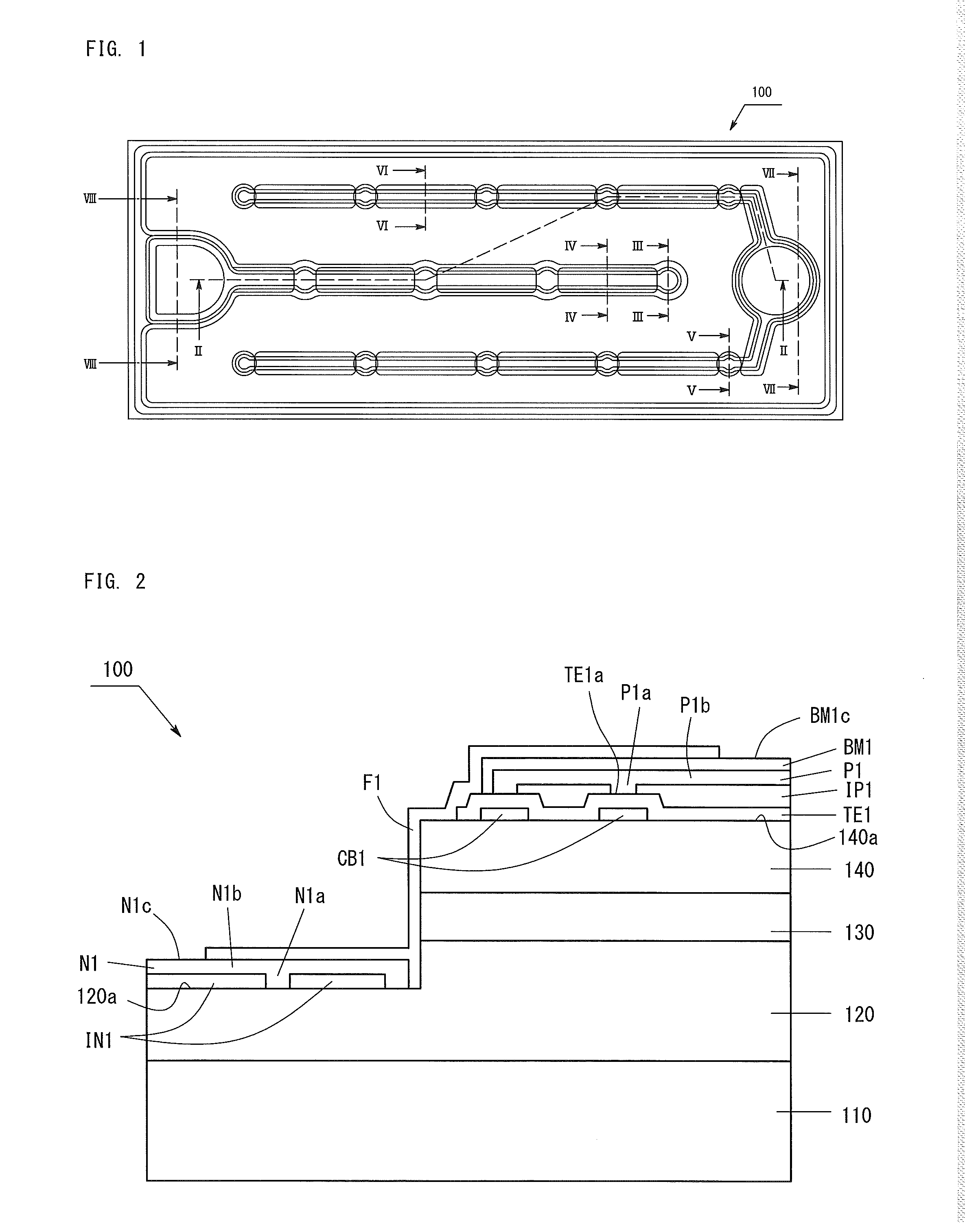
[0084]Next will be described materials of the p-electrode P1, the p-side barrier metal layer BM1, and the n-electrode N1. In Example 1 of Table 1, the p-electrode P1 is formed of α-IZO, Ag alloy, Ta, and Ti deposited in this order on the transparent electrode TEL The thickness of α-IZO is 5 nm. The thickness of Ag alloy is 100 nm. The thickness of Ta is 100 nm. The thickness of Ti is 50 nm. The thicknesses of these layers are merely examples. The thicknesses are not limited to these. Ag alloy is, for example, an alloy containing Ag, Pd, and Cu. Needless to say, any alloy having other composition may also be employed.

[0085]The p-side barrier metal layer BM1 is formed of Ti, Al alloy, Ta, Ti, Pt, Au, and Al deposited in this order on the p-electrode P1. The thickness of Ti is 2 nm. The thickness of Al alloy is 100 nm. The thickness of Ta is 100 nm. The thickness of Ti is 300 nm. The thickness of Pt is 100 nm. The thickness of Au is 1,500 nm. The thickness of Al is 10 n...

example 2

3-2-2. Example 2

[0087]In Example 2 of Table 1, the p-electrode P1 is the same as in Example 1.

[0088]The p-side barrier metal layer BM1 is formed of Ti, Rh, Ti, Au, and Al deposited in this order on the p-electrode P1. The thickness of Ti is 2 nm. The thickness of Rh is 100 nm. The thickness of Ti is 50 nm. The thickness of Au is 1,500 nm. The thickness of Al is 10 nm. The thicknesses of these layers are merely examples. The thicknesses are not limited to these.

[0089]The n-electrode N1 of Example 2 is deposited in the same order as that of the p-side barrier metal layer BM1 of Example 2.

example 3

3-2-3. Example 3

[0090]In Example 3 of Table 1, the p-electrode P1 is formed of Cr, Al alloy, Cr, and Ti deposited in this order on the transparent electrode TEL The thickness of Cr in contact with the transparent electrode TE1 is 2 nm. The thickness of Al alloy is 100 nm. The thickness of Cr is 10 nm. The thickness of Ti is 50 nm. The thicknesses are merely examples. The thicknesses are not limited to these.

[0091]The p-side barrier metal layer BM1 of Example 3 is the same as the p-side barrier metal layer BM1 of Example 3.

[0092]The n-electrode N1 of Example 3 is deposited in the same order as that of the p-side barrier metal layer BM1 of Example 3.

TABLE 1p-side barrier metalp-electrodelayer and n-electrodeExam-Materialα-IZO / Ag alloy / Ta / TiTi / Al alloy / Ta / Ti / Pt / Au / Alple 1Thickness5 / 100 / 100 / 502 / 100 / 100 / 300 / 100 / 1500 / 10(nm)Exam-Materialα-IZO / Ag alloy / Ta / TiTi / Rh / Ti / Au / Alple 2Thickness5 / 100 / 100 / 502 / 100 / 50 / 1500 / 10(nm)Exam-MaterialCr / Al alloy / Cr / TiTi / Rh / Ti / Au / Alple 3Thickness2 / 100 / 10 / 502 / 100 / ...


PUM


Abstract

The present invention provides a Group III nitride semiconductor light-emitting device in which the production method is simplified while migration of at least one of Ag atoms and Al atoms is suppressed, and a production method therefor. The production method comprises steps of forming a first electrode, forming a second electrode, and forming a second electrode side barrier metal layer on the second electrode. Moreover, the second electrode has an electrode layer containing at least one of Ag and Al. In forming the first electrode and the second electrode side barrier metal layer, the second electrode side barrier metal layer is formed on the second electrode while the first electrode to be electrically connected to the first semiconductor layer is formed. The first electrode and the second electrode side barrier metal layer are deposited are deposited in the same layered structure.

Description

BACKGROUND OF THE INVENTION[0001]1. Field of the Invention[0002]The technical field of the present invention relates to a Group III nitride semiconductor light-emitting device and a production method therefor. More specifically, it relates to a Group III nitride semiconductor light-emitting device exhibiting suppression of metal migration and a production method therefor.[0003]2. Background Art[0004]In the Group III nitride semiconductor light-emitting device, a p-electrode or an n-electrode is formed of a metal. Metal includes, for example, Ag or Al which causes migration. Migration refers to a phenomenon in which metal atoms contained in a metal material transfer to the surface or the inside of other material such as insulating member when an electric field is applied to a metal material. Therefore, techniques of suppressing metal migration have been developed.[0005]Japanese Patent Application Laid-Open (kokai) No. 2006-24750 discloses a light-emitting device 8 having an n-type la...

Claims


Application Information

Patent Timeline
IPC IPC(8): H01L33/00H01L33/14H01L33/32H01L33/42H01L33/46H01L33/62
CPCH01L33/0075H01L33/145H01L33/46H01L33/42H01L33/0025H01L33/62H01L33/32H01L33/0095H01L33/38H01L33/405H01L33/44H01L2933/0016
Inventor TOTANI, SHINGO
Owner TOYODA GOSEI CO LTD
Why Eureka
Try Eureka