Circuit module and method of manufacturing same

a technology of circuit modules and circuits, applied in the field of circuit modules, can solve the problems of inability to precisely control the depth of the slits, the shape of the internal shield is limited, and the restriction of the mounting layout of the components, so as to prevent warping and deformation

Active Publication Date: 2016-03-31
KAGA FEI CO LTD
View PDF2 Cites 19 Cited by
  • Summary
  • Abstract
  • Description
  • Claims
  • Application Information

AI Technical Summary

Benefits of technology

[0014]Patent Document 4 discloses a circuit module that has a groove-shaped trench that recesses from the main surface of a sealing body toward a mounting surface, and the trench is formed so that both edges of the trench are shallower than the portion of the trench that extends between the edges (claim 5 of Patent document 4, for example). One of the advantages of the configuration disclosed in Patent Document 4 is that warping and deformation can be prevented.
[0017]Accordingly, the present invention is directed to a scheme that substantially obviates one or more of the above-discussed and other problems due to limitations and disadvantages of the related art. With the above-mentioned situation in mind, an object of the present invention is to provide a circuit module that confers a high degree of design freedom for the shape of the shield; protects the wiring on the circuit board from the radiation of the laser beam; ensures an electrical connection between the wiring and the shield; and facilitates enhancement of shielding capabilities against electromagnetic waves and the like more than the configuration disclosed in Patent Document 4 while also suppressing warping and deformation. Additional problems and effects will be made clear in the detailed description of the invention that will be given later in this specification.

Problems solved by technology

The shape of the internal shield is therefore limited, and there are restrictions to the mounting layout of the components.
Moreover, the depth of the slits cannot be precisely controlled when dicing is used; thus, it is difficult to have the bottom of the slit electrically contact the wiring directly below the slit.
As a result, production costs will increase as the number of components and the number of mounting steps increase.
If the laser beam is too strong, however, it is impossible to avoid damaging the wiring on the circuit board, and if the laser beam is too weak, efficiency decreases and productivity cannot be maintained.
Thus, it can be difficult to set the laser to the optimal strength, which is a problem.

Method used


Image

  • Circuit module and method of manufacturing same
  • Circuit module and method of manufacturing same
  • Circuit module and method of manufacturing same

Examples


Embodiment Construction

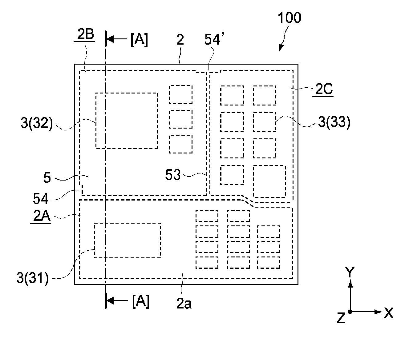
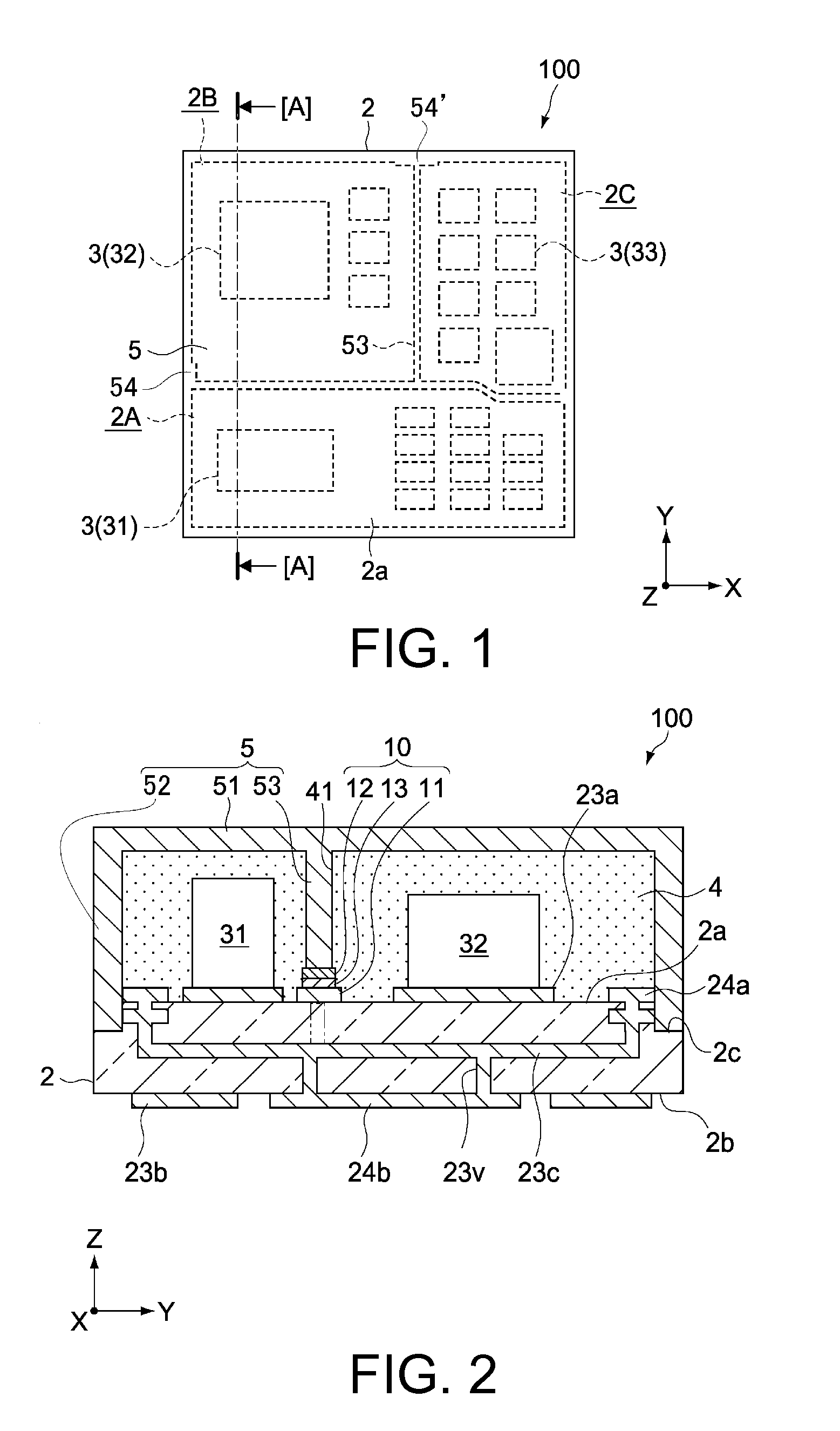
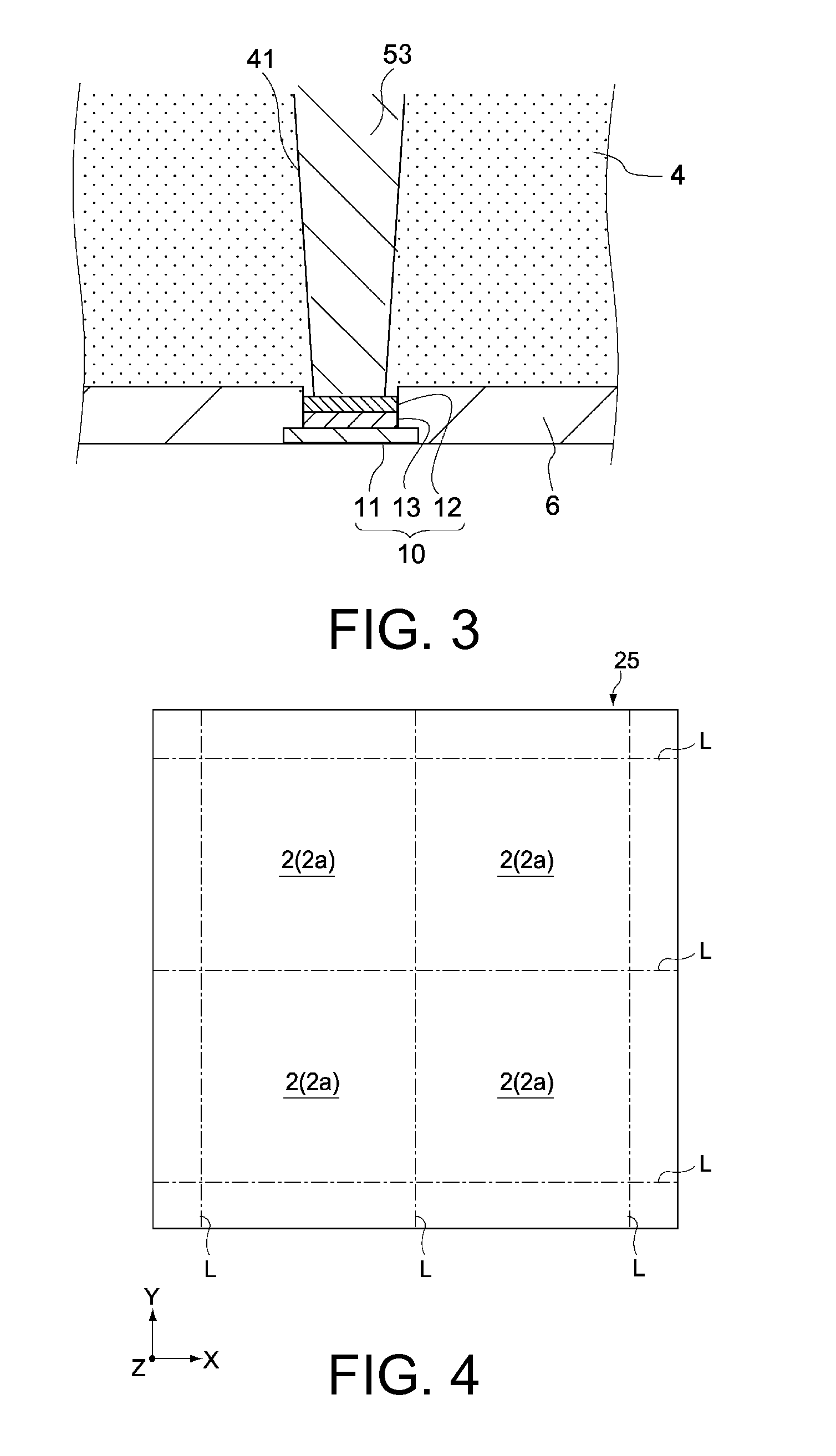
[0038]A circuit module according to an embodiment of the present invention is provided with: a wiring substrate; a plurality of electronic components; a sealing layer; and a conductive shield. The wiring substrate has: a mounting surface that includes a first region and a second region; and a conductive pattern, which is formed along the border of the first region and the second region on the mounting surface and which has the topmost layer thereof made of Au or Ag.

[0039]The plurality of electronic components are mounted in the first region and the second region.

[0040]The sealing layer covers the plurality of electronic components and is formed of an insulating material. The sealing layer has grooves that are formed along the above-mentioned border and that have a depth such that at least a portion of the grooves reaches the topmost layer of the conductive pattern.

[0041]The conductive shield has: a first shielding section that covers the top surface of the sealing layer; a second sh...


PUM


Abstract

A circuit module, including: a substrate having electronic components mounted thereon and further having a conductive pattern that defines respective shielded areas where the electronic components are mounted; a sealing layer covering the substrate and the electronic components, the sealing layer having grooves formed therein along the conductive pattern; and a conductive shield, including: a first shielding section covering a top surface of the sealing layer; a second shielding section covering side faces of the sealing layer; and a third shielding section filling the grooves in the sealing layer, wherein the grooves are shaped such that the third shielding section has at least one end thereof connected to the second shielding section, the third shielding section thereby acting as shielding walls partitioning the respective shielded areas, and that said at least one end of the third shielding section has a width wider than other portions of the third shielding section.

Description

BACKGROUND OF THE INVENTION[0001]1. Technical Field[0002]The present invention relates to a circuit module that has an electromagnetic shielding function and a method of manufacturing the same.[0003]2. Background Art[0004]There are well-known circuit modules in which a plurality of electronic components are mounted on a substrate and the modules are then mounted on various types of electronic devices. This type of circuit module generally has an electromagnetic shielding function that both prevents electromagnetic waves from leaking to the outside of the module and prevents electromagnetic waves from entering into the module from the exterior.[0005]Moreover, as the electronic components mounted within the module have become more diverse along with higher functionality, there have been various techniques proposed for preventing electromagnetic interference among these electronic components. Patent Document 1 discloses a circuit module in which a slit that penetrates a mold resin laye...

Claims


Application Information

Patent Timeline
Patent Type & Authority Applications(United States)
IPC IPC(8): H05K9/00H05K1/02H05K1/18H05K3/28H05K3/30
CPCH05K9/0032H05K1/18H05K2201/0707H05K3/284H05K1/0216H05K3/303H05K2203/107H05K2203/1316H01L2224/16225H01L2924/181H05K3/0052H05K9/0024H05K2201/0715H01L2924/00012
Inventor KITAZAKI, KENZOMUGIYA, EIJISHIMAMURA, MASAYA
Owner KAGA FEI CO LTD
Why Eureka
Try Eureka