Plasma processing apparatus

a processing apparatus and plasma technology, applied in the direction of electrical apparatus, electrical discharge tubes, basic electric elements, etc., can solve the problems of contaminated objects, hardly performed stable etching, etc., to achieve stably etch the object to be processed, suppress the adhesion of non-volatile materials, and hardly changed the supply pattern of material gas

Inactive Publication Date: 2016-04-28
PANASONIC INTELLECTUAL PROPERTY MANAGEMENT CO LTD
View PDF11 Cites 10 Cited by
  • Summary
  • Abstract
  • Description
  • Claims
  • Application Information

AI Technical Summary

Benefits of technology

[0019]According to the plasma processing apparatus of an aspect of the present invention, since the electrode pattern of the electric heater and / or the plate electrode is disposed on the reaction chamber side of the dielectric member, it is possible to efficiently suppress adhesion of the non-volatile material.
[0020]According to the plasma processing apparatus of another aspect of the present invention, since the change of diameter of the gas injection port is suppressed, the supply pattern of the material gas is hardly changed. Consequently, even when the plasma processing is repeatedly performed, it is possible to stably etch the object to be processed. Further, damage to the cover is suppressed, the exchange frequency of the cover can be reduced, and excellent productivity can be obtained.

Problems solved by technology

As a result, the object to be processed may be contaminated.
As a result, a supply pattern of the material gas supplied through the gas injection ports is changed, and stable etching is hardly performed.

Method used


Image

  • Plasma processing apparatus
  • Plasma processing apparatus
  • Plasma processing apparatus

Examples


first embodiment

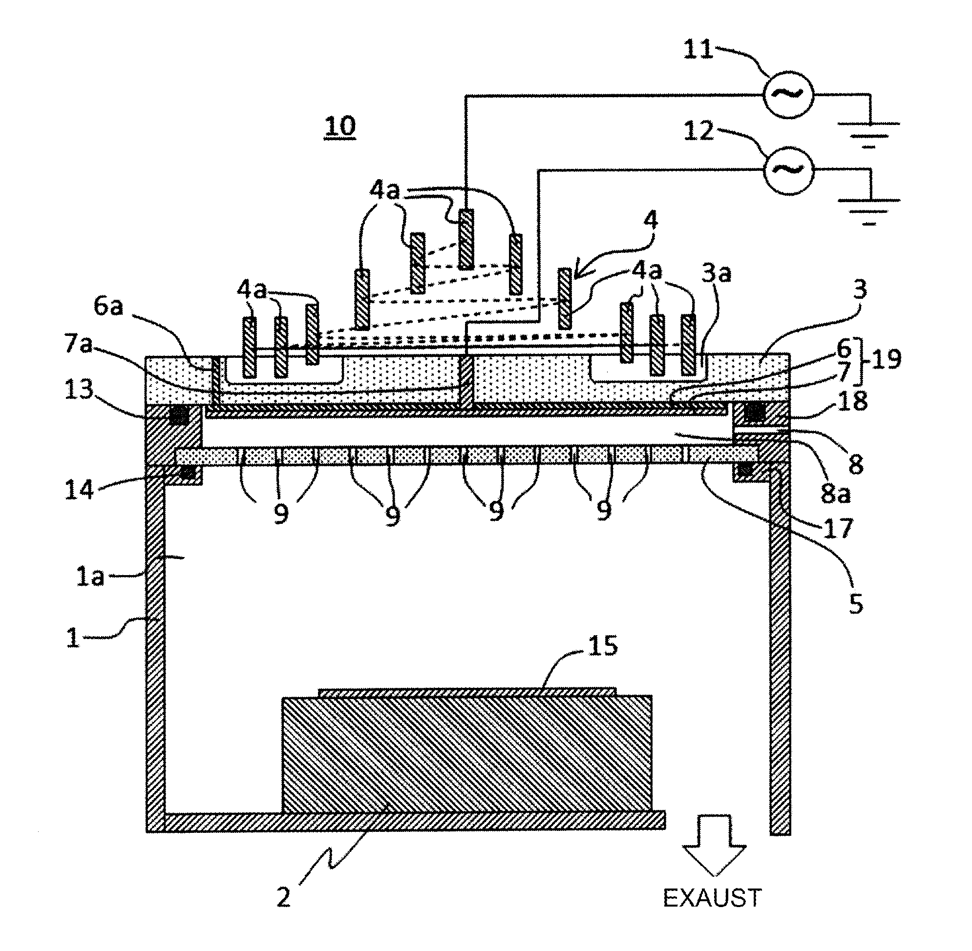
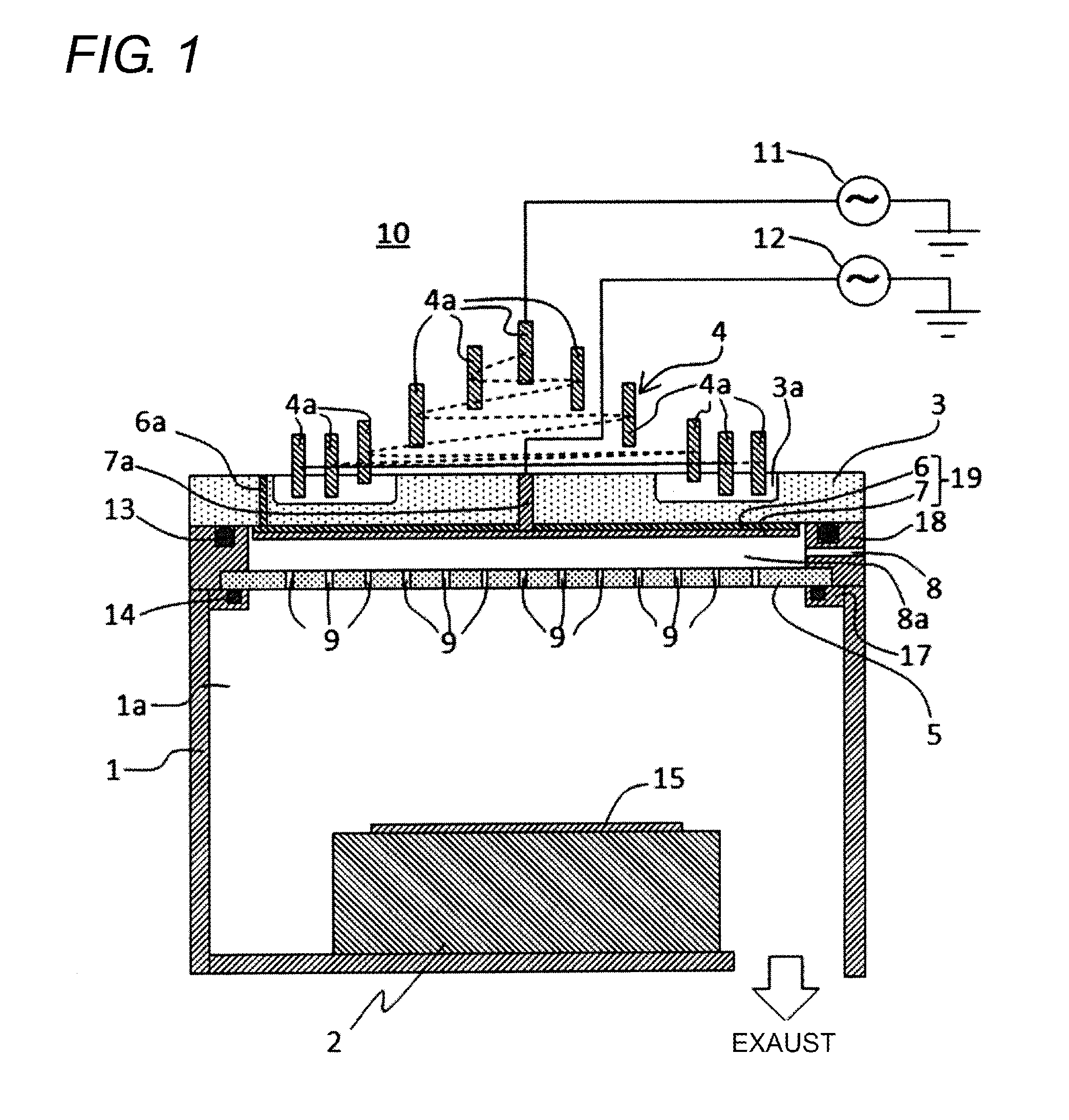
[0043]FIG. 1 shows a structure of a dry etching apparatus 10 of an inductively coupled plasma (ICP) type, which is a plasma processing apparatus according to a first embodiment of the present invention. The dry etching apparatus 10 includes a vessel 1 having a reaction chamber 1a in which an inner atmosphere can be depressurized, a lower electrode 2 which supports a substrate 15 as an object to be processed within the reaction chamber 1a, a dielectric member 3 which closes an opening of the vessel 1 and opposes the substrate 15, and a coil 4 which is disposed on an outer side of the dielectric member 3 opposite to the reaction chamber 1a and generates plasma within the reaction chamber 1a.

[0044]The vessel 1 has a substantially cylindrical shape with an opened top portion. The opening of the top portion is hermetically sealed by the dielectric member 3 as a lid. Atmosphere within the reaction chamber 1a is exhausted by a predetermined pumping device (not shown) and maintained at a d...

second embodiment

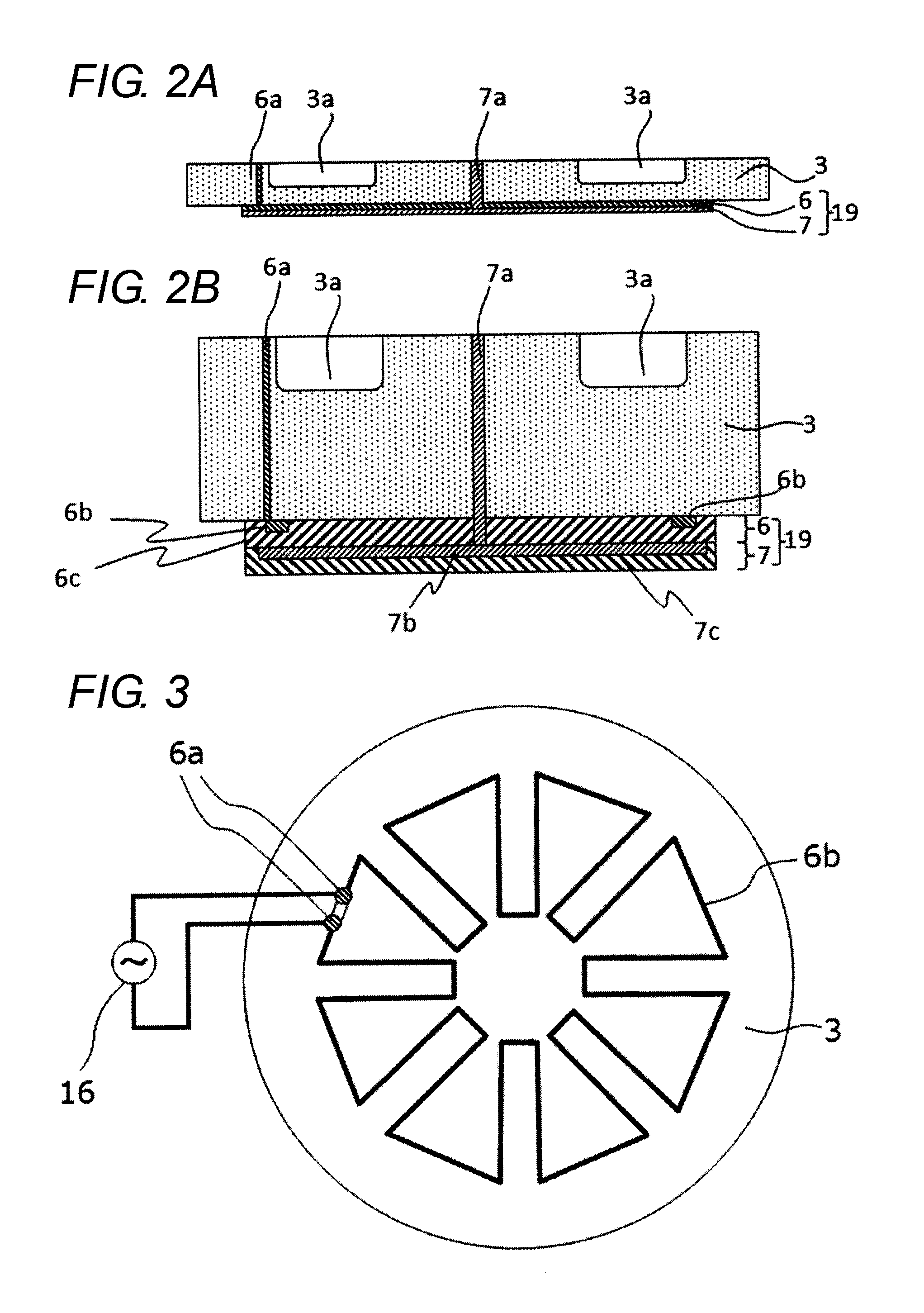
[0088]A plasma processing apparatus according to the present embodiment is the same as that of the first embodiment except that the dielectric member 3 has a recess portion which is provided on the surface on the reaction chamber 1a side (the second surface) and which has a flat bottom surface, and the electrode layer 19 is formed in the recess portion. FIG. 6 is a vertical cross-sectional view schematically showing a structure of a dielectric member 3 and an electrode layer according to the present embodiment. The recess portion is provided in a portion except for a contact region in which the second holder 18 (not shown) contacts the dielectric member 3. Respective constituent elements of this embodiment corresponding to those of the first embodiment are referred to by the common symbols.

[0089]The recess portion can be formed, for example, by machining the second surface of the dielectric member 3. A depth of the recess portion is not limited to a particular size, and may be a siz...

third embodiment

[0091]A plasma processing apparatus according to the present embodiment is the same as that of the first embodiment except for a shape of the groove of the dielectric member and a positional relation between the dielectric member and the coil. FIG. 7A is a vertical cross-sectional view schematically showing an arrangement of a dielectric member and a coil according to the present embodiment. FIG. 7B is a plan view of the dielectric member according to the present embodiment. Respective constituent elements of this embodiment corresponding to those of the first embodiment are referred to by the common symbols. In FIG. 7B, the conductor 4a is omitted for convenience.

[0092]The dielectric member 3 has a circular plate shape. An annular groove 3a is provided in the first surface of the dielectric member 3 such that a center of the annular shape of the groove 3a substantially overlaps with the center of the coil 4 in plan view. The groove 3a includes: a first groove portion 3x having a la...


PUM


Abstract

A plasma processing apparatus includes: a vessel which includes a reaction chamber, atmosphere within the reaction chamber capable of being depressurized; a lower electrode which supports an object to be processed within the reaction chamber; a dielectric member which comprises a first surface and a second surface opposite to the first surface, and which closes an opening of the vessel such that the first surface opposes an outside of the reaction chamber and the second surface opposes the object to be processed; and a coil which opposes the first surface of the dielectric member, and which generates plasma within the reaction chamber. An electrode pattern and an insulation film which covers the electrode pattern are formed on the second surface of the dielectric member.

Description

CROSS-REFERENCE TO RELATED APPLICATION(S)[0001]This application is based on and claims priority from Japanese Patent Application No. 2014-215147 filed on Oct. 22, 2014 and Japanese Patent Application No. 2015-020415 filed on Feb. 4, 2015, the entire contents of which are incorporated herein by reference.BACKGROUND[0002]1. Field of the Invention[0003]One or more embodiments of the present invention relate to a plasma processing apparatus of an inductively coupled plasma (ICP) type, for example, a plasma processing apparatus used for manufacturing semiconductor elements or electric components.[0004]2. Description of Related Art[0005]A plasma processing apparatus an inductively coupled plasma (ICP) type generates a dielectric magnetic field by supplying radio frequency power from a radio frequency power supply to an induction coil disposed outside a reaction chamber. The dielectric magnetic field passes through a dielectric member which closes an opening of the reaction chamber, and ac...

Claims


Application Information

Patent Timeline
Patent Type & Authority Applications(United States)
IPC IPC(8): H01L21/683
CPCH01L21/6831H01J37/321H01J37/32119H01J37/32522
Inventor IWAI, TETSUHIROOKITA, SHOGOWATANABE, SYOUZOU
Owner PANASONIC INTELLECTUAL PROPERTY MANAGEMENT CO LTD
Why Eureka
Try Eureka