

Wafer level packaging approach for semiconductor devices
- Summary
- Abstract
- Description
- Claims
- Application Information
AI Technical Summary
Benefits of technology
Problems solved by technology
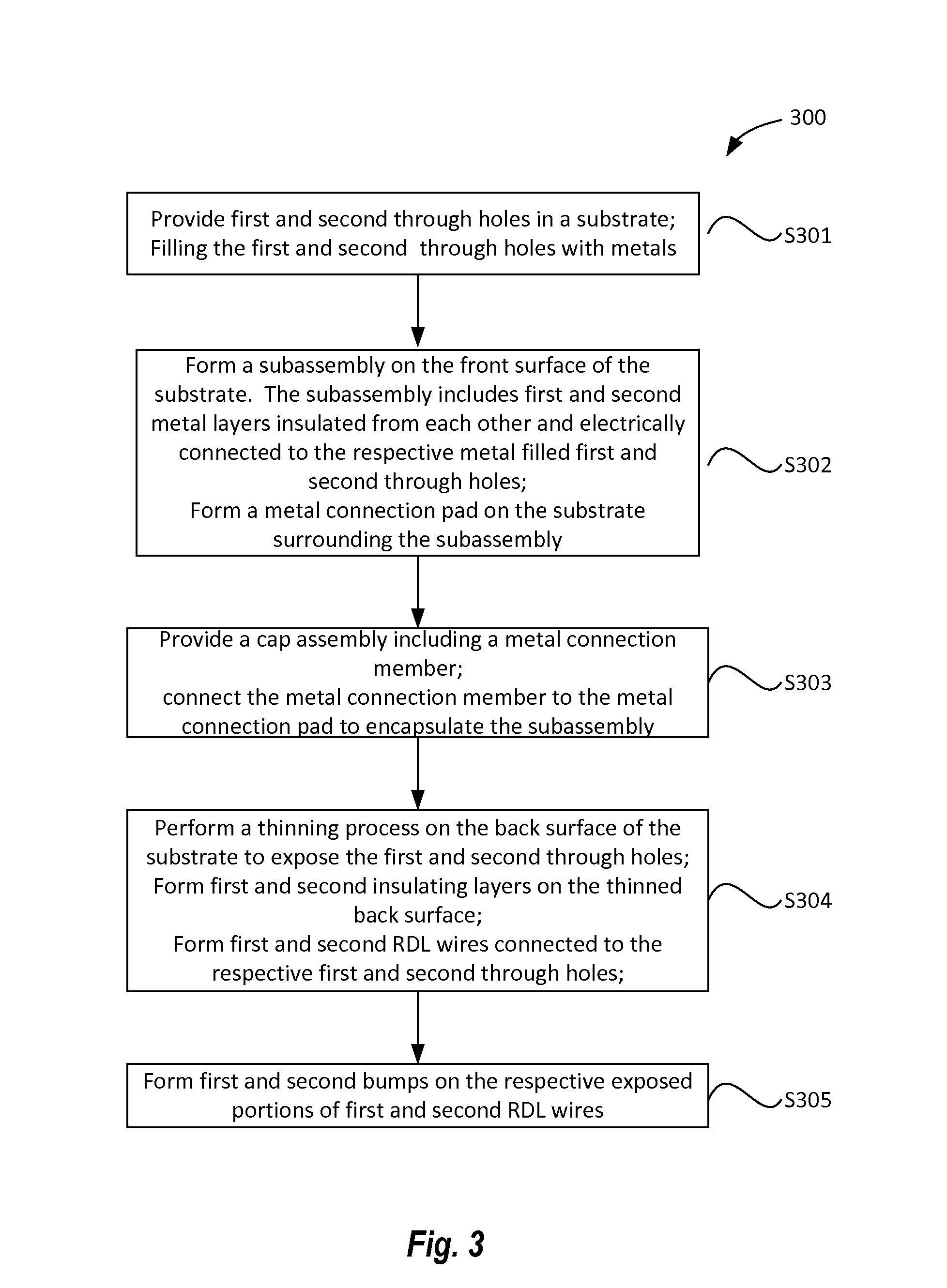
Method used
Image

Examples
Embodiment Construction
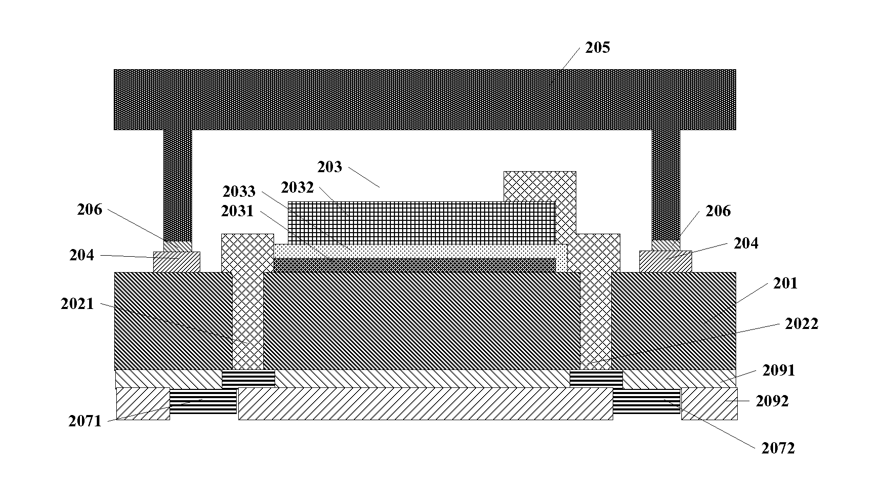
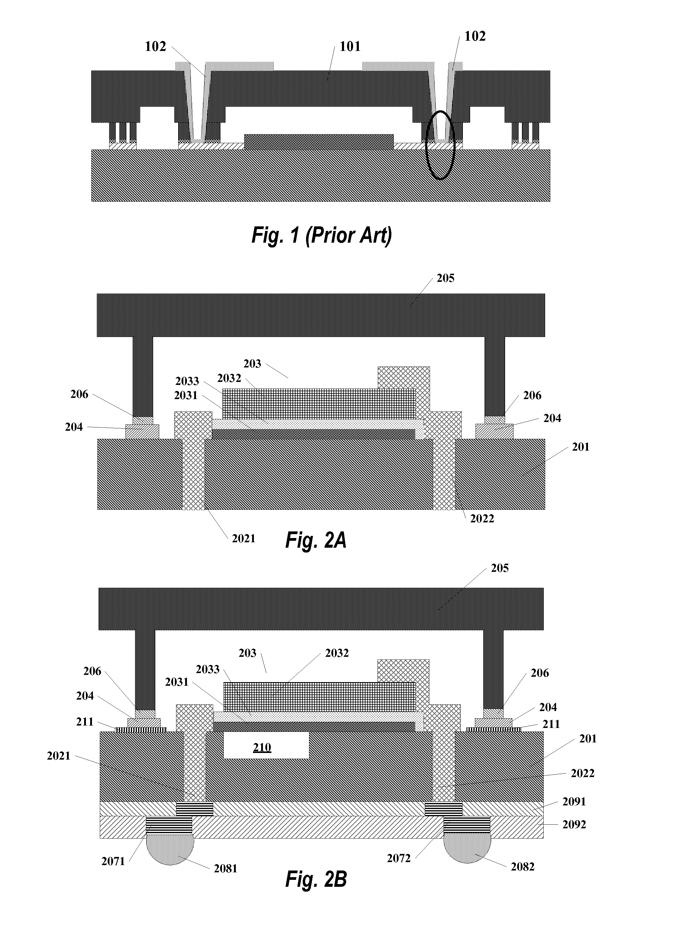
[0056]The present invention will be described with respect to particular embodiments and with reference to certain drawings, but the invention is not limited thereto but only by the claims. It is noted that, unless otherwise specified, the relative arrangement of elements and steps set forth in the embodiments, numeric expressions and values shall not be construed as limiting the scope of the present invention.
[0057]The drawings described are only schematic and are non-limiting. In the drawings, the size of some of the elements may be exaggerated and not drawn to scale for illustrative purposes.
[0058]The following description of at least one embodiment is merely illustrative, and should not construed as limiting the present invention and its applications or use.
[0059]Method and devices known to people of skill in the art will not be discussed in detail for the sake of brevity. The conventional known techniques, methods and equipment should be considered as part of this disclosure.
[0...
PUM
 Abstract
Description
Claims
Application Information