

Imaging Lens, and Electronic Apparatus Including the Same
- Summary
- Abstract
- Description
- Claims
- Application Information
AI Technical Summary
Benefits of technology
Problems solved by technology
Method used
Image

Examples
first embodiment
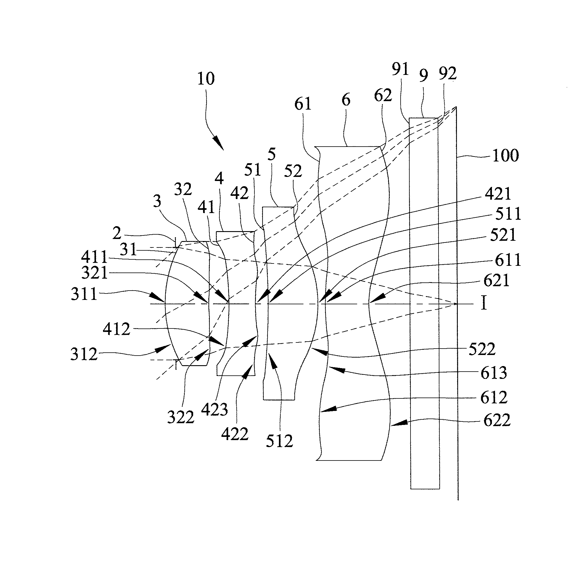
[0054]Referring to FIG. 6, an imaging lens 10 according to the present disclosure includes an aperture stop 2, a first lens element 3, a second lens element 4, a third lens element 5, a fourth lens element 6 and an optical filter 9 arranged in the given order along an optical axis (I) from an object side to an image side. The optical filter 9 is an infrared cut filter for selectively absorbing infrared light to thereby reduce imperfection of images formed at an image plane 100.
[0055]Each of the first, second, third and fourth lens elements 3-6 and the optical filter 9 has an object-side surface 31, 41, 51, 61, 91 facing toward the object side, and an image-side surface 32, 42, 52, 62, 92 facing toward the image side. Light entering the imaging lens 10 travels through the aperture stop 2, the object-side and image-side surfaces 31, 32 of the first lens element 3, the object-side and image-side surfaces 41, 42 of the second lens element 4, the object-side and image-side surfaces 51, 5...
second embodiment
[0104]Shown in FIG. 11 is a table that lists values of some optical data corresponding to the surfaces 31-61 and 91, 32-62 and 92 of the The imaging lens 10 has an overall system focal length of 1.558 mm, an HFOV of 40.079°, an F-number of 2.056, and a system length of 2.104 mm.
[0105]Shown in FIG. 12 is a table that lists values of some aspherical coefficients of the aforementioned relationship (1) corresponding to the second embodiment.
[0106]Relationships among some of the aforementioned lens parameters corresponding to the second embodiment are listed in columns of FIGS. 26 and 27 corresponding to the second embodiment.
[0107]FIGS. 13(A) to 13(D) respectively show simulation results corresponding to longitudinal spherical aberration, sagittal astigmatism aberration, tangential astigmatism aberration, and distortion aberration of the second embodiment. It can be understood from FIGS. 13(A) to 13(D) that the second embodiment is able to achieve a relatively good optical performance....
third embodiment
[0110]Shown in FIG. 15 is a table that lists values of some optical data corresponding to the surfaces 31-61 and 91, 32-62 and 92 of the The imaging lens 10 has an overall system focal length of 1.539 mm, an HFOV of 40.345°, an F-number of 2.056, and a system length of 2.081 mm.
[0111]Shown in FIG. 16 is a table that lists values of some aspherical coefficients of the aforementioned relationship (1) corresponding to the third embodiment.
[0112]Relationships among some of the aforementioned lens parameters corresponding to the third embodiment are listed in columns of FIGS. 26 and 27 corresponding to the third embodiment.
[0113]FIGS. 17(A) to 17(D) respectively show simulation results corresponding to longitudinal spherical aberration, sagittal astigmatism aberration, tangential astigmatism aberration, and distortion aberration of the third embodiment. It can be understood from FIGS. 17(A) to 17(D) that the third embodiment is able to achieve a relatively good optical performance.
[0114...
PUM
 Abstract
Description
Claims
Application Information