Multi-Electrode Photonic Digital To Analog Converting Vector Modulator

a vector modulator and photonic digital technology, applied in the field of optical communication, can solve the problems of destructive and constructive, and achieve the effect of reducing the need for differential amplifiers and low power consumption

Inactive Publication Date: 2016-05-19
ALCATEL LUCENT SAS
View PDF3 Cites 23 Cited by
  • Summary
  • Abstract
  • Description
  • Claims
  • Application Information

AI Technical Summary

Benefits of technology

[0013]In particular a Digital Signal Processor (DSP) generates the modulation signals, which are passed through differential driver amplifiers whose outputs are connected to the electrodes positioned proximate each of the waveguide paths of each sub-Mach-Zehnder modulator. The outputs of the differential driver amplifiers provide balanced modulation signals (i.e., differential signals) that are inverted with respect to each other to provide a the push-pull type signal. The modulation signals from the DSP can be digital, analog, or discrete time signals obtained from sampling an analog signal. In another embodiment, the DSP can generate the differential signals eliminating the need for the differential driver amplifiers. The electrodes can be designed such that their bandwidths can be made substantially equal to each other, and thus can be linearly equalized as needed. Different digital drive signal levels can be used to obtain a chain of power-of-two phase shifts within each modulator irrespective of individual lengths of the electrodes. Any other suitable electrode ladder with non-power-of-two ratios may be constructed as well.
[0014]When the modulation signal is a digital signal, a quantization bit can be generated using several electrodes so that multiple electrodes contribute to the phase shift of that one quantization bit. Because several electrodes can be combined to generate the voltage level of one quantization bit, the need for differential amplifiers can be eliminated. As a result, relatively low power consumption technologies such as CMOS technology can be used to construct the modulator and the overall digital-electronic-to-analog-optical converter.

Problems solved by technology

Portions of the optical wave signal travel from the start point through the pair of sub-paths to the end point and said portions interfere (destructively, constructively, or in any suitable intermediate manner) with each other at the end point.

Method used


Image

  • Multi-Electrode Photonic Digital To Analog Converting Vector Modulator
  • Multi-Electrode Photonic Digital To Analog Converting Vector Modulator
  • Multi-Electrode Photonic Digital To Analog Converting Vector Modulator

Examples


Embodiment Construction

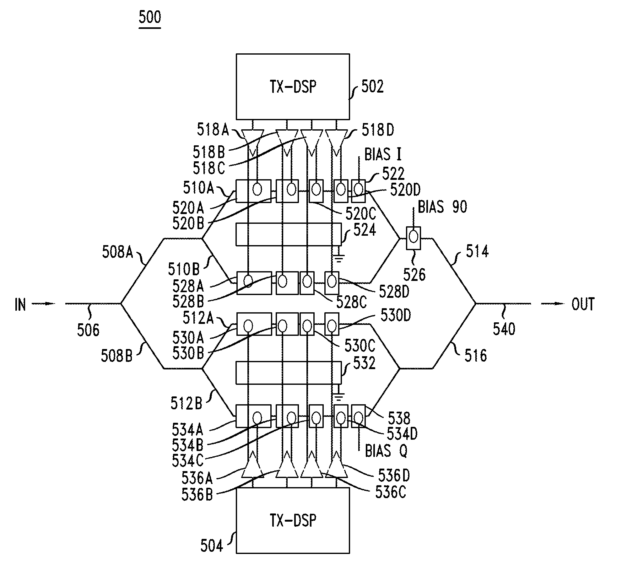
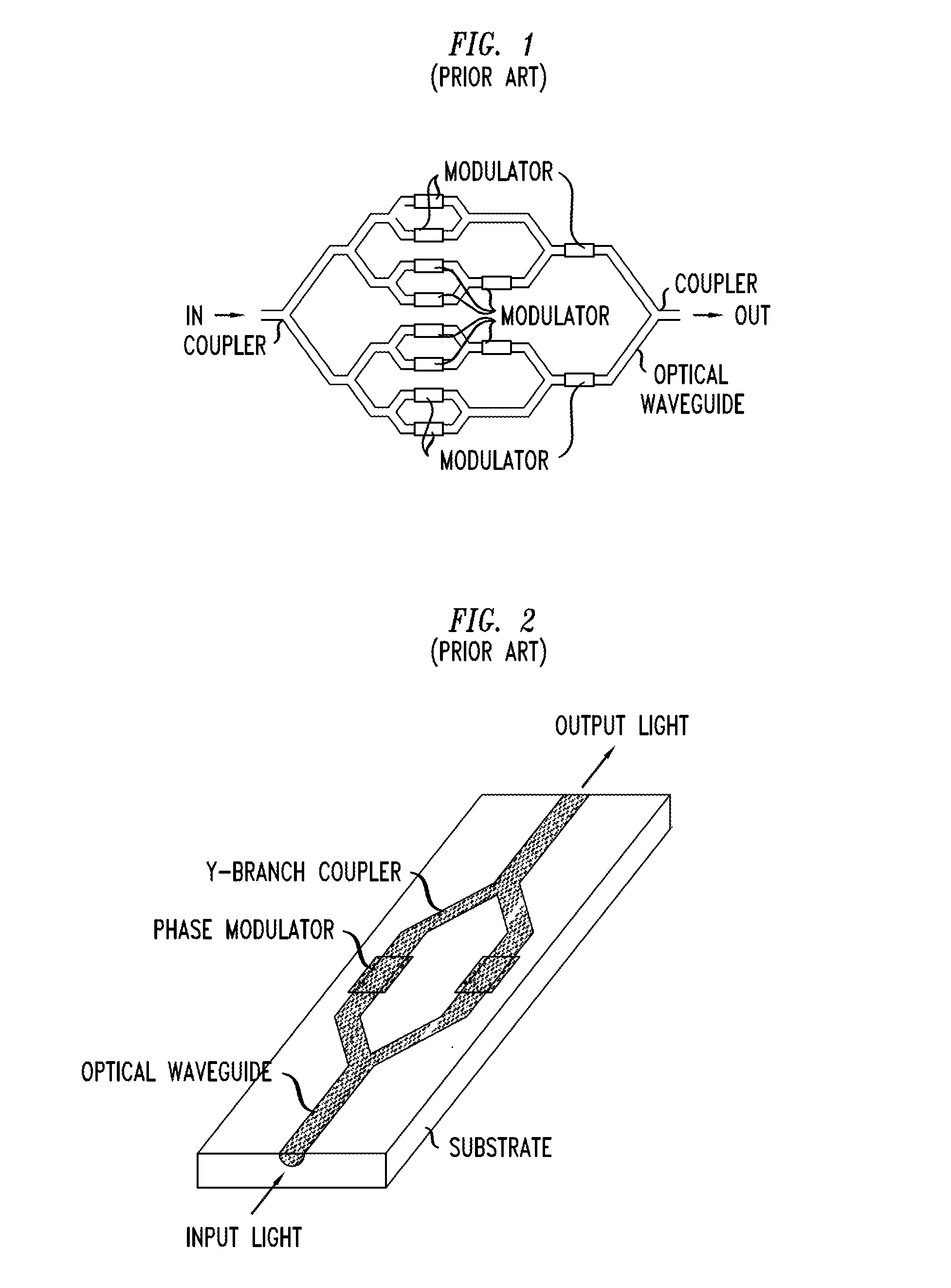
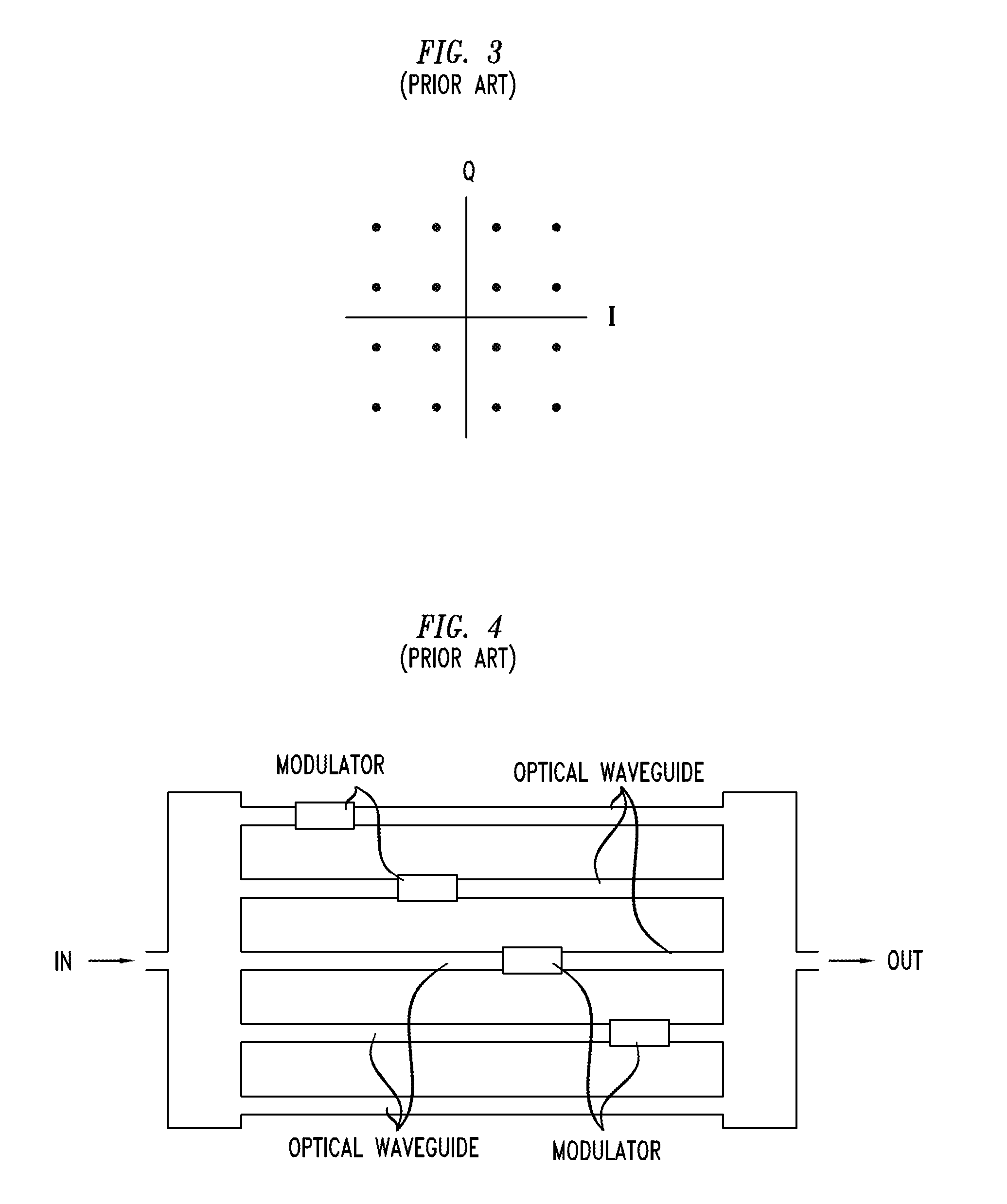
[0023]The present invention provides a digital-electronic-to-analog-optical converter comprising two main waveguide paths coupled to each other at a start point and at an end point where each main waveguide path comprises a coupled pair of sub-paths having a first common end and a second common end connected to the start point and end point respectively. The converter further comprises a plurality of modulating signal emitters positioned proximate the sub-paths to modulate an optical wave signal (causing one or more phase shifts) traveling within the sub-path pairs with differential signals generated based on either a differential signal source or the position of the modulating signal emitters relative to the sub-paths. Portions of the optical wave signal travel from the start point through the pair of sub-paths to the end point and said portions interfere (destructively, constructively, or in any suitable intermediate manner) with each other at the end point.

[0024]A transmit signal...


PUM

PropertyMeasurementUnit
phase shiftsaaaaaaaaaa
phaseaaaaaaaaaa
discrete timeaaaaaaaaaa

Abstract

A digital-electronic-to-analog-optical converter, which has a structure consistent with a super-Mach-Zehnder interferometer, and which can perform the functionalities of both a Digital to Analog Converter (DAC) and a digital modulator uses a sub-Mach-Zender modulator to modulate optical wave signals propagating through its optical waveguide in a push-pull manner. The modulation performed is phase modulation realized with electrodes positioned near the optical wave guide where such electrodes carry modulation signals in digital, analog or discrete time signal format creating electromagnetic or electric fields that engage the optical wave signals traveling through the waveguide thus imparting a phase shift onto the optical wave signals. The amount of the phase shift can be implemented through the geometry of the electrodes, the length of time the modulating signal is applied, and the amplitude of the modulating signal.

Description

FIELD OF THE INVENTION[0001]The present invention generally relates to optical communications and specifically to a device for modulating an optical wave using digital modulation techniques.BACKGROUND OF THE INVENTION[0002]In optical communication systems, digital to analog conversion (DAC) is an important feature of modern high speed optical transponders that are used for various purposes including the generation of higher order modulation formats (e.g., Quadrature Amplitude Modulation or QAM), digital pulse shaping (Nyquist pulses, root raised cosine pulse shaping), or the pre-distortion of transmit signals to compensate for certain transmission impairments (e.g., fiber nonlinearity) that occur within optical fiber media. At the transmission end of many optical communication systems that use digital modulation techniques, DACs are used as part of the modulation circuitry. Typically, the circuit architecture used for many such digital modulation circuitry comprises a Digital Signal...

Claims


Application Information

Patent Timeline
Patent Type & Authority Applications(United States)
IPC IPC(8): G02F1/225G02F7/00
CPCG02F1/2257G02F2001/212G02F7/00G02F1/2255H04B10/5053H04B10/541H04B10/556G02F1/212
Inventor WINZER, PETER J.SETHUMADAVAN, CHANDRASEKHARRAYBON, GREGORY
Owner ALCATEL LUCENT SAS
Why Eureka
Try Eureka