Semiconductor Device, Manufacturing Method of Semiconductor Device, and Electronic Device

a semiconductor and semiconductor technology, applied in the direction of semiconductors, electrical devices, transistors, etc., can solve the problems of poor electrical characteristics and poor electrical characteristics, and achieve the effects of reducing the amount of oxygen vacancies in reducing the amount of interface states in the vicinity of the oxide semiconductor layer, and favorable electrical characteristics

Inactive Publication Date: 2016-06-09
SEMICON ENERGY LAB CO LTD
View PDF8 Cites 40 Cited by
  • Summary
  • Abstract
  • Description
  • Claims
  • Application Information

AI Technical Summary

Benefits of technology

[0027]According to one embodiment of the present invention, a semiconductor device in which the amount of oxygen vacancies in an oxide semiconductor layer can be reduced, a semiconductor device in which the amount of interface states in the vicinity of the oxide semiconductor layer can be reduced, a semiconductor device having favorable electrical characteristics, a semiconductor device having high reliability, a semiconductor device with low power consumption, a semiconductor device that can be manufactured in a simple process, a novel semiconductor device or the like, or a manufacturing method of the semiconductor device can be provided.

Problems solved by technology

An increase in oxygen vacancies in an oxide semiconductor layer can cause poor electrical characteristics in some cases; for example, the transistor becomes normally-on, leakage current increases, or threshold voltage is shifted due to stress application.
It is also known that there are some causes of variation in electrical characteristics other than oxygen vacancies; for example, an interface state or the existence of impurities in the vicinity of a channel can cause poor electrical characteristics.

Method used


Image

  • Semiconductor Device, Manufacturing Method of Semiconductor Device, and Electronic Device
  • Semiconductor Device, Manufacturing Method of Semiconductor Device, and Electronic Device
  • Semiconductor Device, Manufacturing Method of Semiconductor Device, and Electronic Device

Examples


embodiment 1

[0101]In this embodiment, a semiconductor device which is one embodiment of the present invention and its manufacturing method is described with reference to drawings.

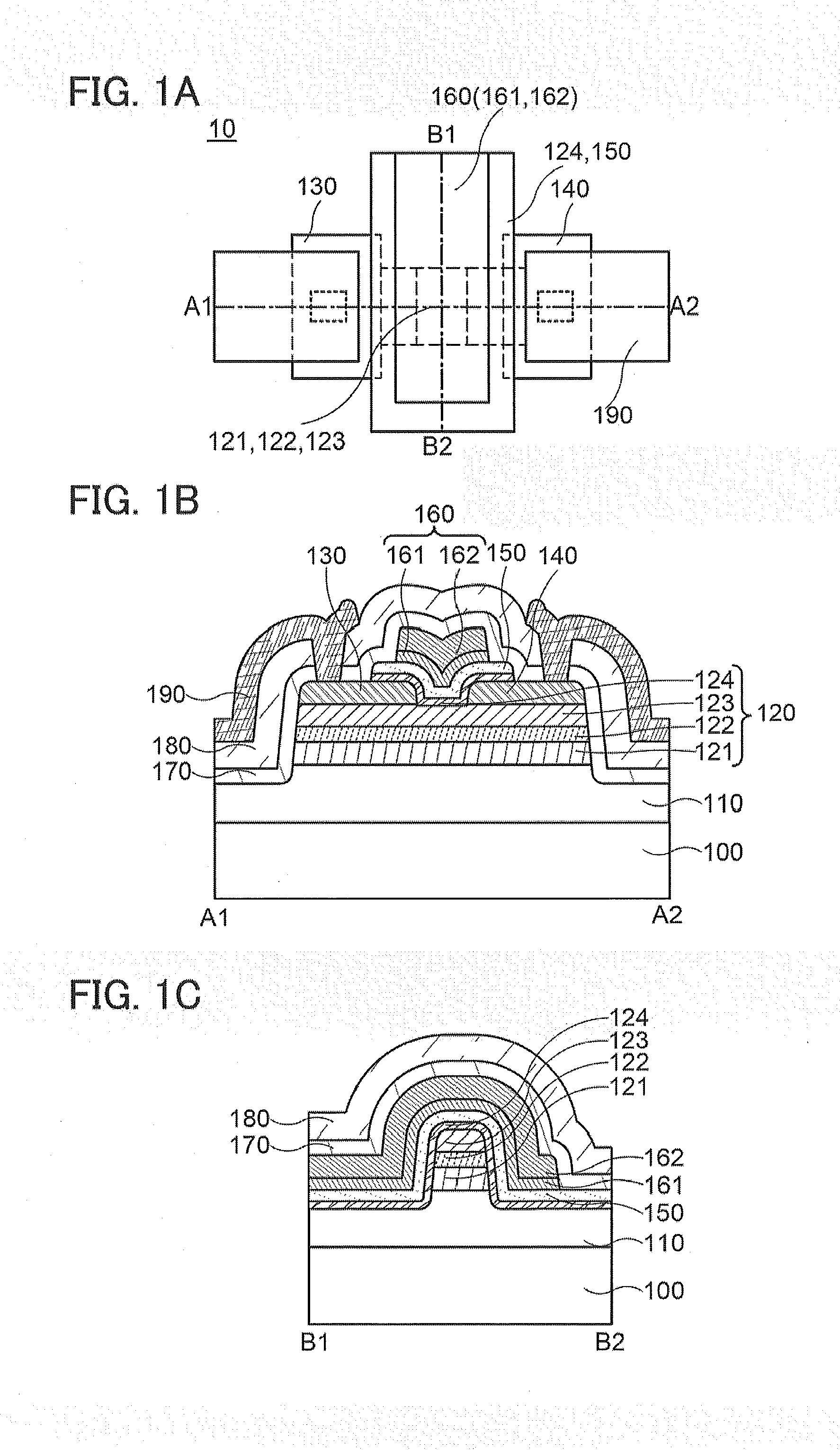
[0102]FIGS. 1A to 1C are a top view and cross-sectional views of a transistor 10 of one embodiment of the present invention: FIG. 1A is a top view, FIG. 1B is a cross-sectional view taken along dashed-dotted line A1-A2 in FIG. 1A, and FIG. 1C is a cross-sectional view taken along dashed-dotted line B1-B2 in FIG. 1A. Note that in FIG. 1A, some components are scaled up or down in size or omitted for easy understanding. The directions of dashed-dotted lines A1-A2 and B1-B2 can be referred to as a channel length direction and a channel width direction, respectively.

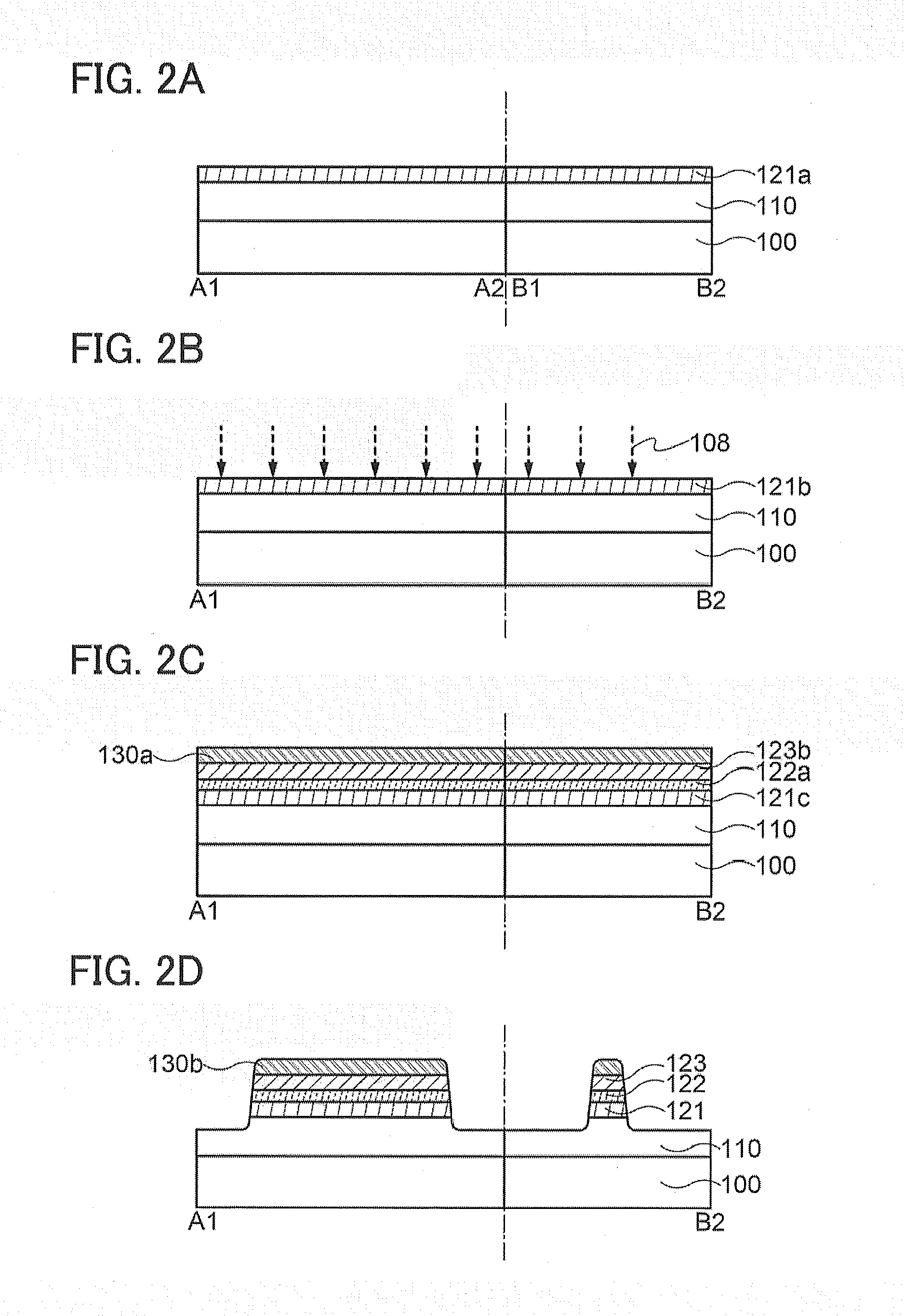
[0103]The transistor 10 includes an insulating layer 110 over a substrate 100; an oxide semiconductor layer 121, an oxide semiconductor layer 122, and an oxide semiconductor layer 123 over the insulating layer 110; a source electrode layer 130 and a drain electr...

embodiment 2

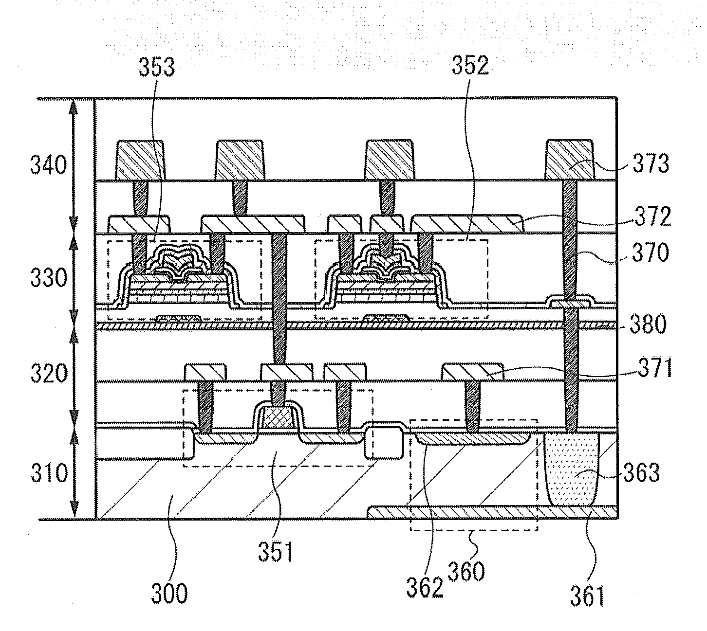
[0307]In this embodiment, a transistor having a structure which is different from the structures of the transistor 10, the transistor 11, the transistor 12, and the transistor 13 described in Embodiment 1 and a method for manufacturing the transistor will be described.

[0308]FIGS. 14A, 14B, and 14C are a top view and cross-sectional views of a transistor 14 of one embodiment of the present invention. FIG. 14A is a top view. FIG. 14B is a cross-sectional view taken along dashed-dotted line A1-A2 in FIG. 14A. FIG. 14C is a cross-sectional view taken along dashed-dotted line B1-B2 in FIG. 14A. In FIG. 14A, some components are scaled up or down in size or omitted for easy understanding. In addition, the direction of dashed-dotted line A1-A2 and the direction of dashed-dotted line B1-B2 are sometimes referred to as a channel length direction and a channel width direction, respectively.

[0309]The transistor 14 shown in FIGS. 14A, 14B, and 14C includes an insulating layer 171 under the insul...

embodiment 3

[0322]High integration of a semiconductor device requires miniaturization of a transistor. However, it is known that miniaturization of a transistor causes deterioration of electrical characteristics of the transistor. A decrease in channel width causes a reduction in on-state current.

[0323]In the transistor of one embodiment of the present invention shown in FIGS. 1A to 1C, for example, as described above, the third oxide semiconductor layer 123 is formed so as to cover the oxide semiconductor layer 123 where a channel is formed and the channel formation layer and the gate insulating film are not in contact with each other. Accordingly, scattering of carriers at the interface between the channel formation layer and the gate insulating layer can be reduced and the on-state current of the transistor can be increased.

[0324]In the transistor of one embodiment of the present invention, the gate electrode layer 161 and the gate electrode layer 162 are formed to electrically surround the ...


PUM


Abstract

Provided is a semiconductor device which can suppress an increase in oxygen vacancies in an oxide semiconductor layer and a manufacturing method of the semiconductor device. The semiconductor device includes a first oxide semiconductor layer over the first insulating layer; a second oxide semiconductor layer over the first oxide semiconductor layer; a third oxide semiconductor layer over the second oxide semiconductor layer; a source electrode layer and a drain electrode layer each over the third oxide semiconductor layer; a fourth semiconductor layer over the source and drain electrode layers, and the third oxide semiconductor layer; a gate insulating layer over the fourth oxide semiconductor layer; a gate electrode layer over the gate electrode layer and overlapping with the source and drain electrode layers, and the fourth oxide semiconductor layer; and a second insulating layer over the first insulating layer, and the source, gate, and drain electrode layers.

Description

BACKGROUND OF THE INVENTION[0001]1. Field of the Invention[0002]The present invention relates to an object, a method, or a manufacturing method. The present invention relates to a process, a machine, manufacture, or a composition of matter. In particular, the present invention relates to, for example, a semiconductor device, a display device, a light-emitting device, a power storage device, an imaging device, a driving method thereof, or a manufacturing method thereof. In particular, one embodiment of the present invention relates to a semiconductor device or a manufacturing method of the semiconductor device.[0003]In this specification and the like, a semiconductor device generally means a device that can function by utilizing semiconductor characteristics. A transistor and a semiconductor circuit are embodiments of semiconductor devices. In some cases, a storage device, a display device, or an electronic device includes a semiconductor device.[0004]2. Description of the Related Ar...

Claims


Application Information

Patent Timeline
Patent Type & Authority Applications(United States)
IPC IPC(8): H01L29/786H01L21/02H01L21/467H01L29/66H01L21/4763
CPCH01L29/7869H01L29/78696H01L29/78606H01L29/66969H01L21/0228H01L21/467H01L21/02266H01L21/02178H01L21/47635H01L21/02554H01L21/02565H01L21/02631H01L27/1207H01L27/1225H01L27/1248
Inventor ITO, DAIGOISHIYAMA, TAKAHISAHANAOKA, KAZUYA
Owner SEMICON ENERGY LAB CO LTD
Why Eureka
Try Eureka