Flexible display device with multiple types of micro-coating layers

a display device and micro-coating technology, applied in the field of electronic devices with a display, can solve the problems of unforgiving margin of errors, new challenges that need to be solved, and components formed directly on the base substrate along with display pixels tend to have tremendously small dimensions, so as to reduce or eliminate the inactive area and minimize the inactive area

Active Publication Date: 2016-06-16
LG DISPLAY CO LTD
View PDF3 Cites 128 Cited by
  • Summary
  • Abstract
  • Description
  • Claims
  • Application Information

AI Technical Summary

Benefits of technology

[0008]Accordingly, it is desirable to bend the base substrate where the display area and the inactive area are formed thereon. This would allow even some of the inactive area to be positioned behind the active area of the display panel, thereby reducing or eliminating the inactive area that needs to be hidden under the masking or the device housing. Not only does the bending of the base substrate will minimize the inactive area size need to be hidden from view, but it will also open possibility to various new display device designs.
[0010]As such, various factors and special parameters must be taken in consideration in designing a flexible display. An aspect of the present disclosure is related to a flexible display, which includes configurations for wire traces to withstand bend stress for reliable operation of the flexible display.
[0014]In some embodiments, the first micro-coating layer underneath the second micro-coating layer is coated over at least some part of the encapsulation. The first micro-coating layer may also be extended further and provided over at least some part of the printed circuit film at the opposite end of the bend allowance section. In some embodiments, the first micro-coating layer coated over the bend allowance section may be overflowed onto both the part of the encapsulation and the part of the printed circuit film. The first micro-coating layer coated on the part of the encapsulation and / or the printed circuit film can provide stronger adhesion to the encapsulation and / or the printed circuit film for improved sealing at the respective areas.
[0015]In some cases, the second micro-coating layer on the first micro-coating layer may provide stronger adhesion with the surface of the encapsulation and / or the printed circuit film than the first micro-coating layer. Accordingly, in some embodiments, the second micro-coating layer on the first micro-coating layer may be coated over at least some part of the encapsulation and / or at least some part of the printed circuit film.
[0018]In one suitable embodiment, the flexible display apparatus includes a base layer with a display area and a non-display area. A plurality of organic light-emitting diode (OLED) elements is disposed in the display area, and an encapsulation is provided on the plurality of OLED elements. The flexible display apparatus further includes a printed circuit film, which is attached to the base layer at the non-display area. The base layer is curved inwardly or outwardly such that a bend allowance section is provided between the encapsulation and the printed circuit. One or more wire traces are routed in the bend allowance section. In the area between the encapsulation and the printed circuit, at least two regions, which are coated with different type of micro-coating layer from each other, are provided to suppress separation of micro-coating layers from the coated surface and to suppress permeation of moisture.

Problems solved by technology

However, there are various new challenges that need to be solved in providing such flexible displays.
The components formed directly on the base substrate along with the display pixels tend to have tremendously small dimensions with unforgiving margin of errors.
Further, these components need to be formed on extremely thin sheet to provide flexibility, making those components extremely fragile to various mechanical and environmental stresses instigated during the manufacture and / or in the use of the displays.
If care is not taken, the mechanical stresses from bending of the flexible display can negatively affect the reliability or even result in complete component failure.
Even a micro-scale defect in the component thereof can have devastating effects on the performance and / or reliability of the display pixels amounting to scrap the entire display panel without an option to repair.
On the other hand, simply increasing the bending radius to ease the bend stress may make it difficult to garner any significant benefits in bending the base substrate of the display panel.

Method used


Image

  • Flexible display device with multiple types of micro-coating layers
  • Flexible display device with multiple types of micro-coating layers
  • Flexible display device with multiple types of micro-coating layers

Examples


Embodiment Construction

Flexible Display

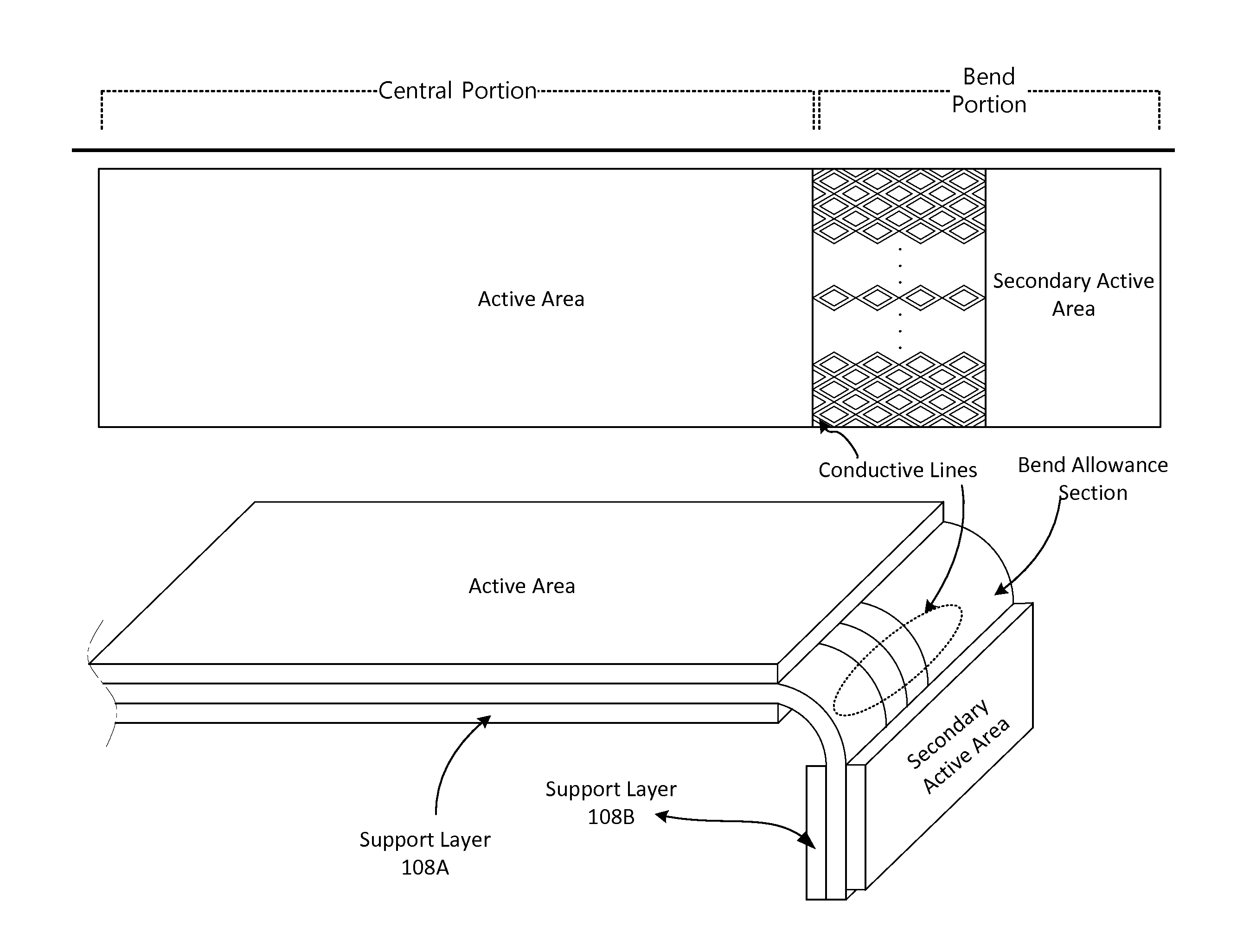
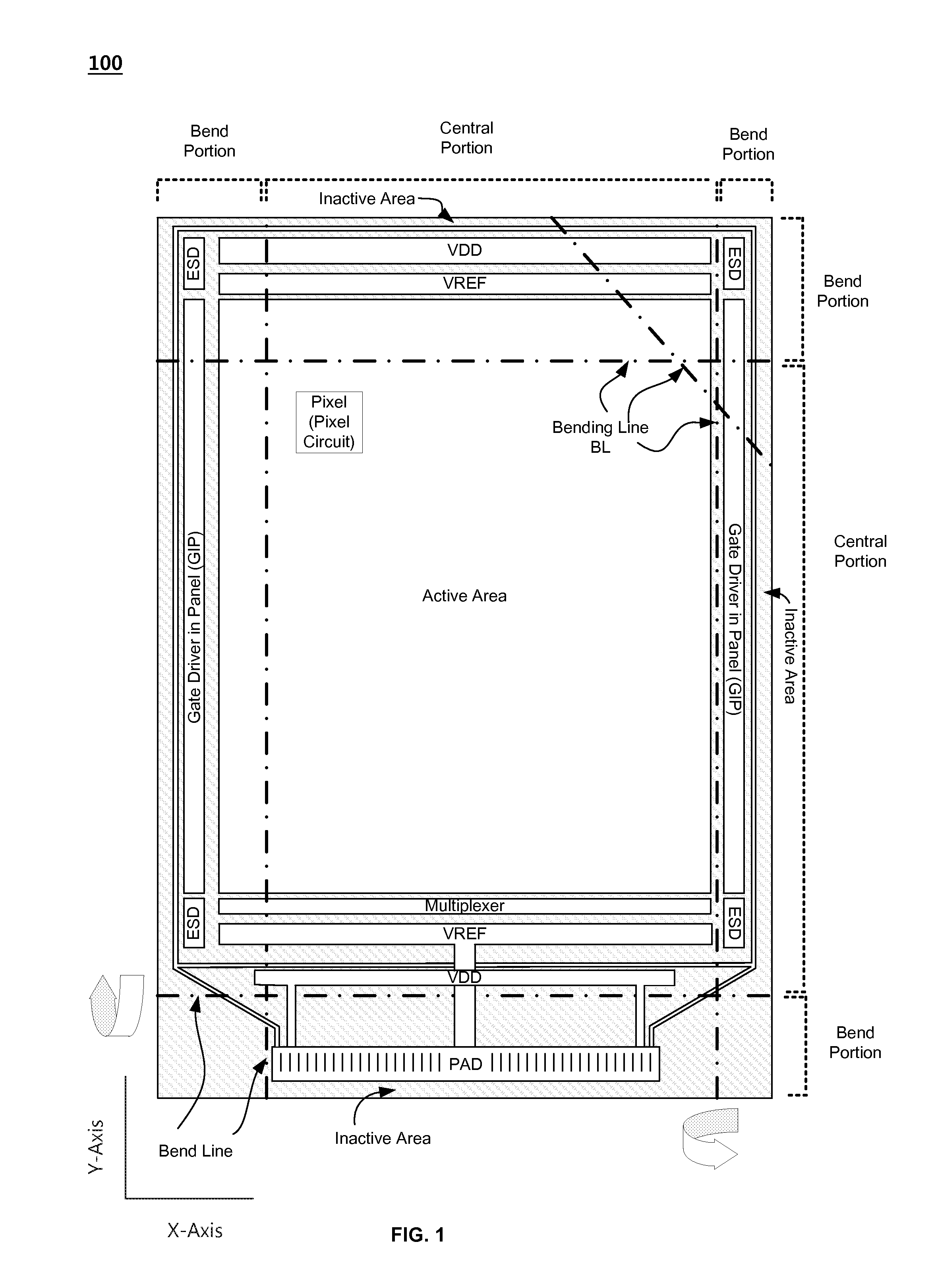
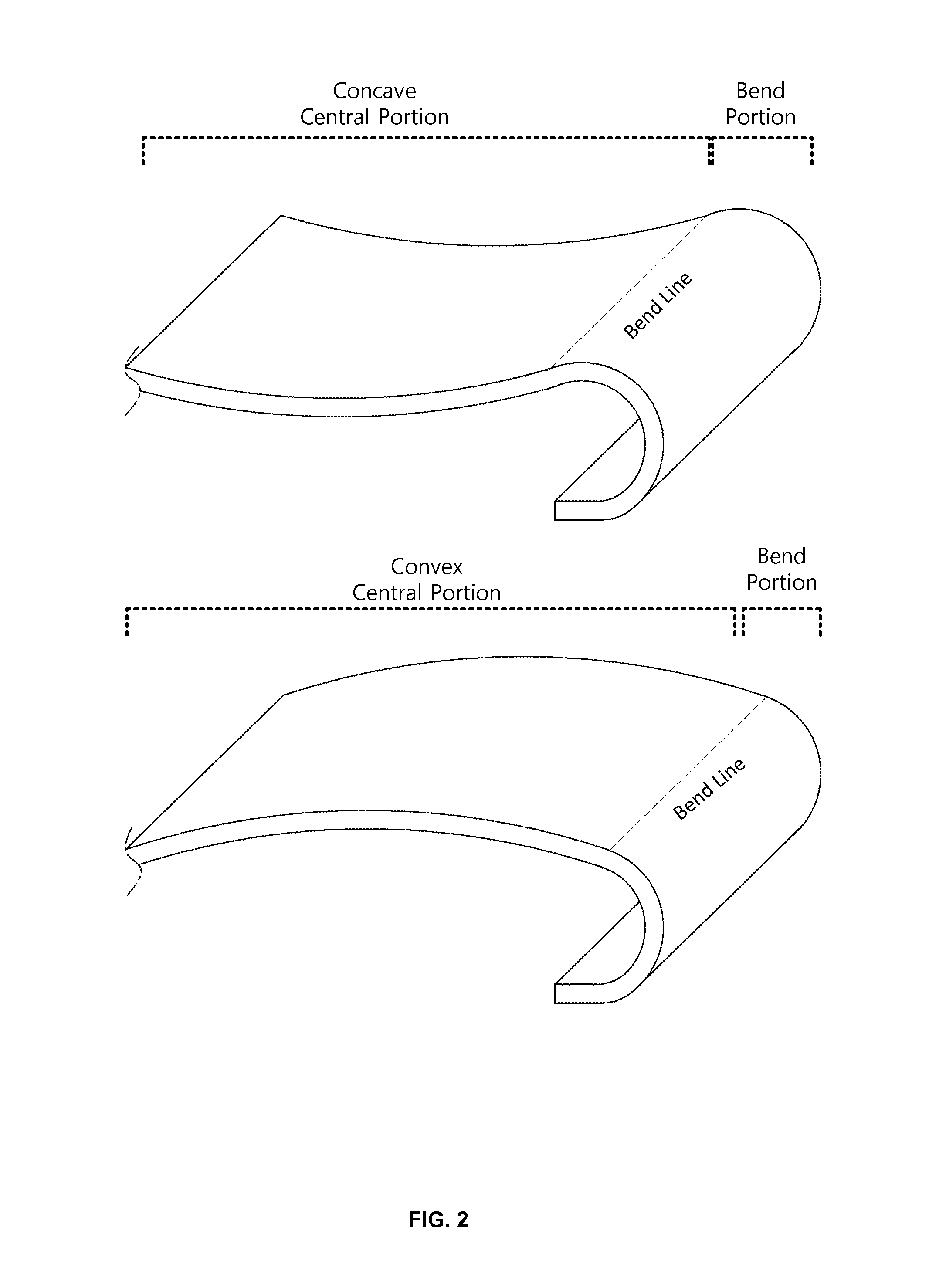
[0043]FIG. 1 illustrates exemplary flexible display 100 which may be incorporated in electronic devices. Referring to FIG. 1, the flexible display 100 includes at least one active area (i.e., display area), in which an array of display pixels are formed therein. One or more inactive areas may be provided at the periphery of the active area. That is, the inactive area may be adjacent to one or more sides of the active area. In FIG. 1, the inactive area surrounds a rectangular shape active area. However, it should be appreciated that the shapes of the active area and the arrangement of the inactive area adjacent to the active area are not particularly limited as the exemplary flexible display 100 illustrated in FIG. 1. The active area and the inactive area may be in any shape suitable to the design of the electronic device employing the flexible display 100. Non-limiting examples of the active area shapes in the flexible display 100 include a pentagonal shape, a hexago...


PUM


Abstract

There is provided a flexible display having a plurality of innovations configured to allow bending of a portion or portions to reduce apparent border size and / or utilize the side surface of an assembled flexible display.

Description

BACKGROUND[0001]1. Technical Field[0002]This relates generally to electronic devices, and more particularly, to electronic devices with a display.[0003]2. Description of the Related Art[0004]Electronic devices often include displays. For example, cellular telephones and portable computers include displays for presenting information to a user. Components for the electronic device, including but not limited to a display, may be mounted in a plastic or a metal housing.[0005]An assembled display may include a display panel and a number of components for providing a variety of functionalities. For instance, one or more display driving circuits for controlling the display panel may be included in a display assembly. Examples of the driving circuits include gate drivers, emission (source) drivers, power (VDD) routing, electrostatic discharge (ESD) circuits, multiplex (mux) circuits, data signal lines, cathode contacts, and other functional elements. There may be a number of peripheral circ...

Claims


Application Information

Patent Timeline
Patent Type & Authority Applications(United States)
IPC IPC(8): H05B33/04H05B33/06
CPCH05B33/06H05B33/04H10K59/131H10K77/111H10K50/841H10K50/868H10K50/86H10K50/844H10K2102/311Y02P70/50H10K50/846Y02E10/549
Inventor KIM, SUNGWOOCHOI, SIEHYUGPARK, JEHONGLEE, YEASLEKIM, CHIWOONG
Owner LG DISPLAY CO LTD
Why Eureka
Try Eureka