

Leadframe package with pre-applied filler material
a technology of filler material and lead frame, which is applied in the direction of electrical apparatus construction details, printed circuit non-printed electric components association, and semiconductor/solid-state device details, etc., can solve the problems of further limited space for solder joints, weakened solder joints between the package and the pcb
- Summary
- Abstract
- Description
- Claims
- Application Information
AI Technical Summary
Benefits of technology
Problems solved by technology
Method used
Image

Examples
Embodiment Construction
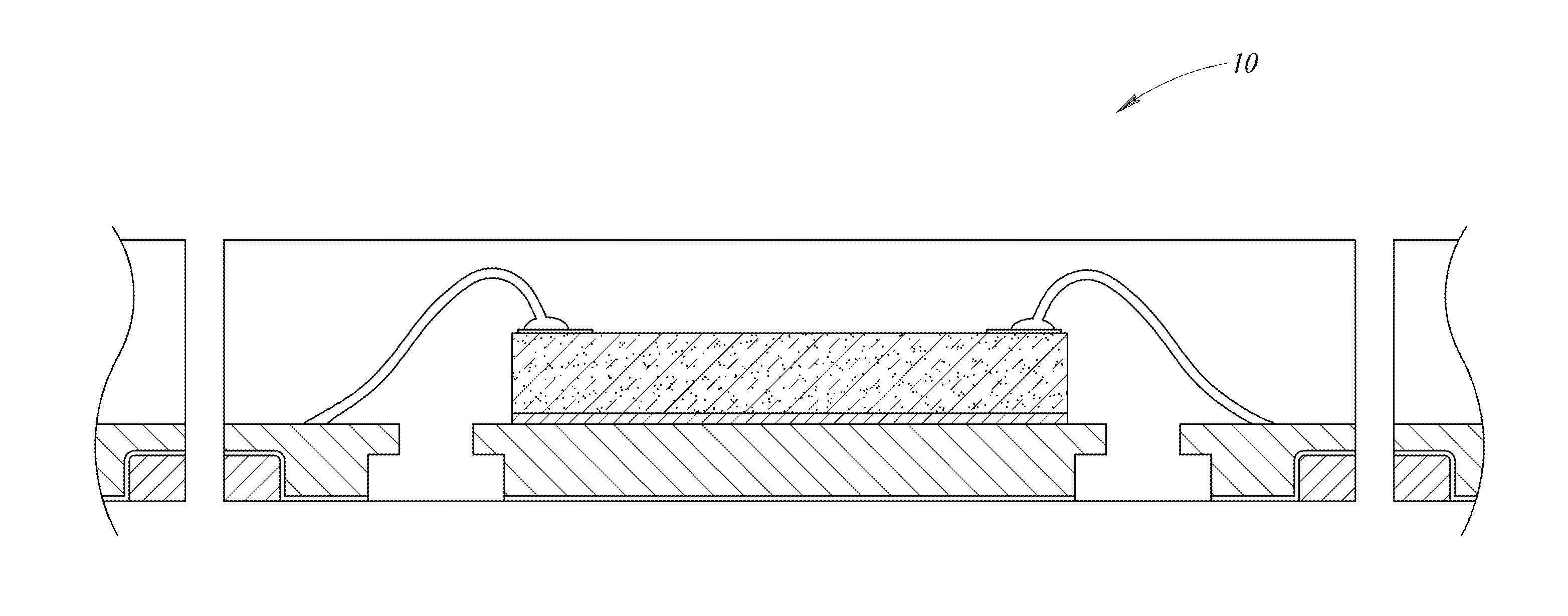
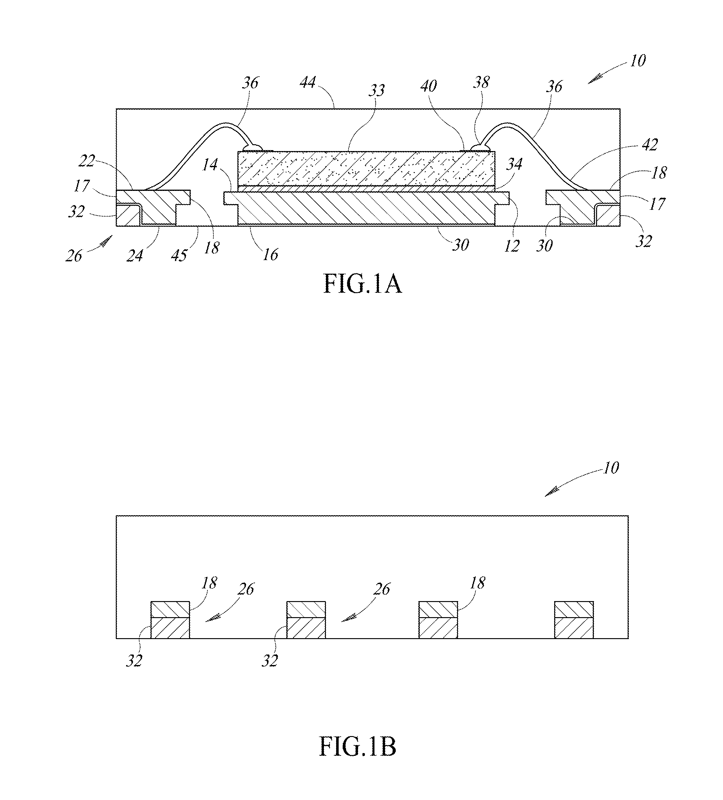
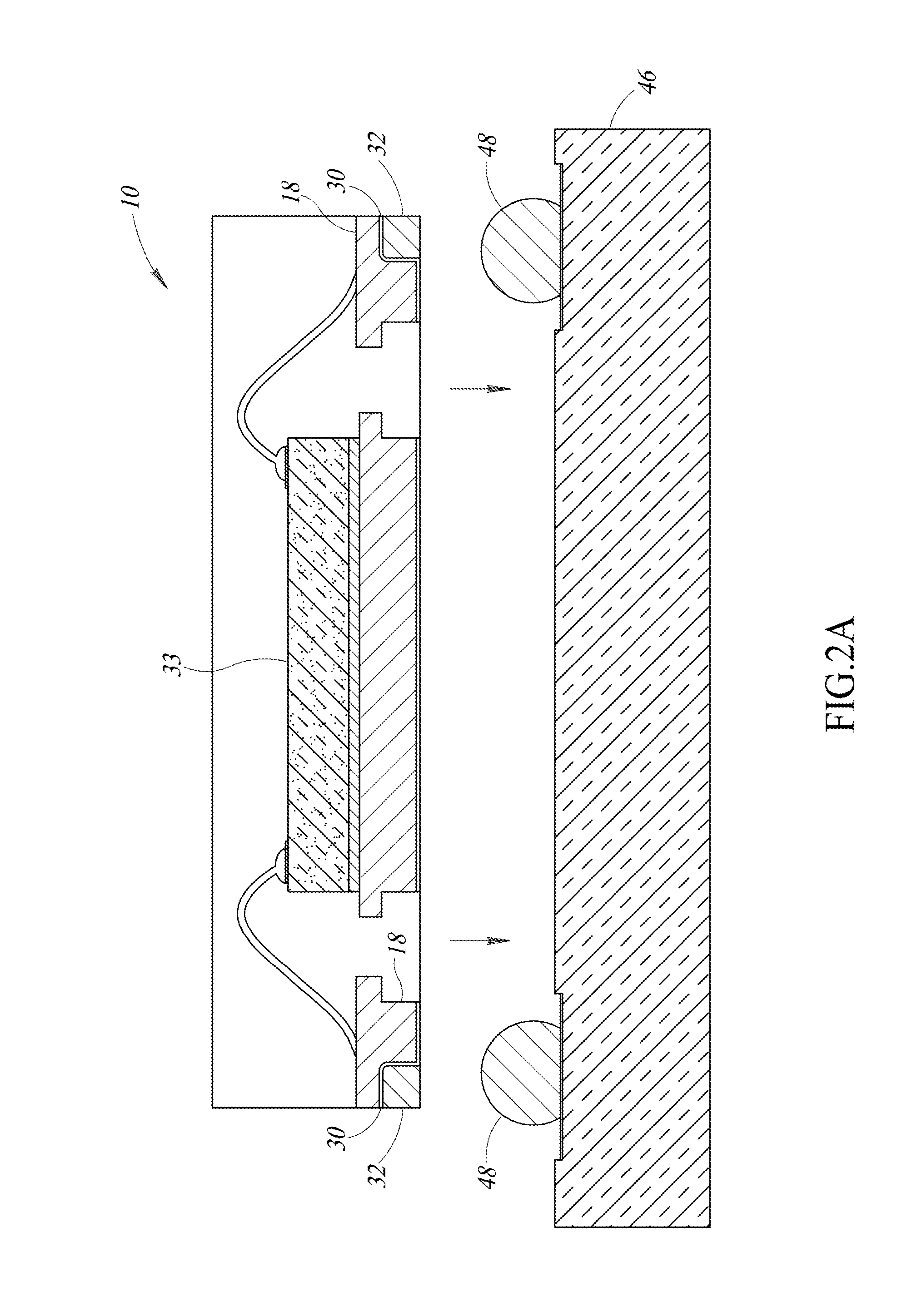
[0014]FIG. 1A shows a cross-sectional view of a leadframe package 10 made in accordance with one embodiment of the disclosure. The package 10 shows a die pad 12 and two leads 18 located spaced apart from and on opposing sides of the die pad 12. The die pad 12 has upper and lower surfaces 14, 16 and the leads 18 have upper and lower surfaces 22, 24. The lower surfaces 24 of the leads 18 may also be referred to as lands of the package 10. The die pad 12 and the leads 18 are made of a conductive material, such as copper or a copper alloy.
[0015]FIG. 1B shows a side view of the package 10. As shown by the side view, the package includes four leads 18 on one side. It is to be appreciated, however, that any number of leads may be included in the package including one lead on just one side of the die pad 12. In some embodiments, the leads are provided on two sides or four sides of the die pad.
[0016]An outer surface 17 and the lower surface 24 of the leads 18 have respective recesses 26 form...
PUM
 Abstract
Description
Claims
Application Information