Organic light emitting diode display

a light-emitting diode and display technology, applied in semiconductor devices, instruments, computing, etc., can solve the problems of affecting the voltage of the driving gate node of the driving transistor, reducing a process design, and reducing the parasitic capacitance between the driving connecting member and the data line, so as to reduce the height of the driving connecting member and prevent the effect of parasitic capacitan

Active Publication Date: 2016-07-21
SAMSUNG DISPLAY CO LTD
View PDF9 Cites 34 Cited by
  • Summary
  • Abstract
  • Description
  • Claims
  • Application Information

AI Technical Summary

Benefits of technology

[0029]According to embodiments of the present disclosure, by positioning the shielding member, which is connected to the second storage electrode which is a portion of the driving voltage line, between the driving connecting member and the data line, parasitic capacitance between the driving connecting member and the data line may be reduced or prevented.
[0030]Also, by forming the shielding opening, formed by removing a portion of the second gate insulating layer under the driving connecting member, to lower the height of the driving connecting member above the substrate, the distance between the data line and the driving connecting member is increased such that the parasitic capacitance between the driving connecting member and the data line may be reduced or minimized.
[0031]Accordingly, kickback voltage due to t

Problems solved by technology

However, due to parasitic capacitance formed between the driving gate node connected to the driving gate electrode of the driving transistor and the data line, a voltage change of the data line (e.g., a change in the voltage transmitted by the data line) affects the voltage of the driving gate node of the driving transistor.
To reduce or prevent this phenomenon, a dis

Method used


Image

  • Organic light emitting diode display
  • Organic light emitting diode display
  • Organic light emitting diode display

Examples


Embodiment Construction

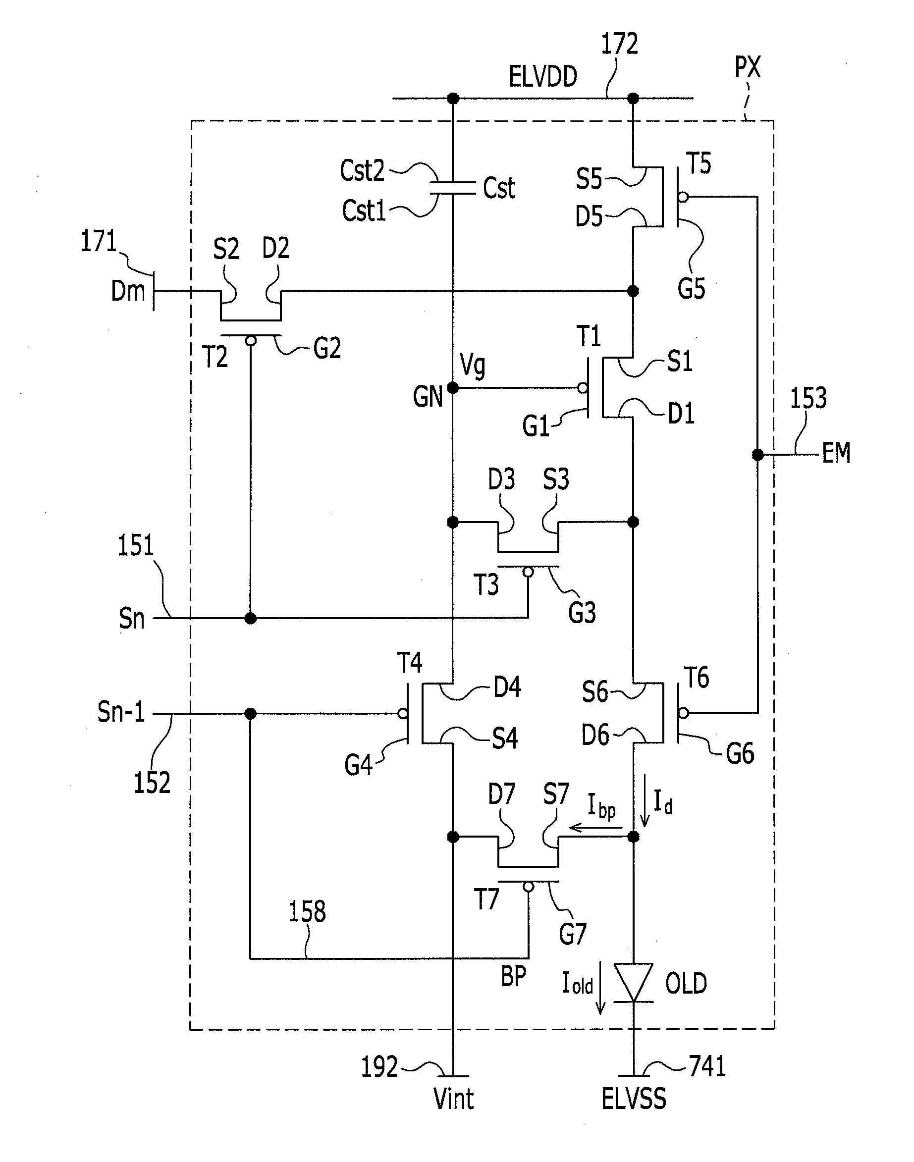
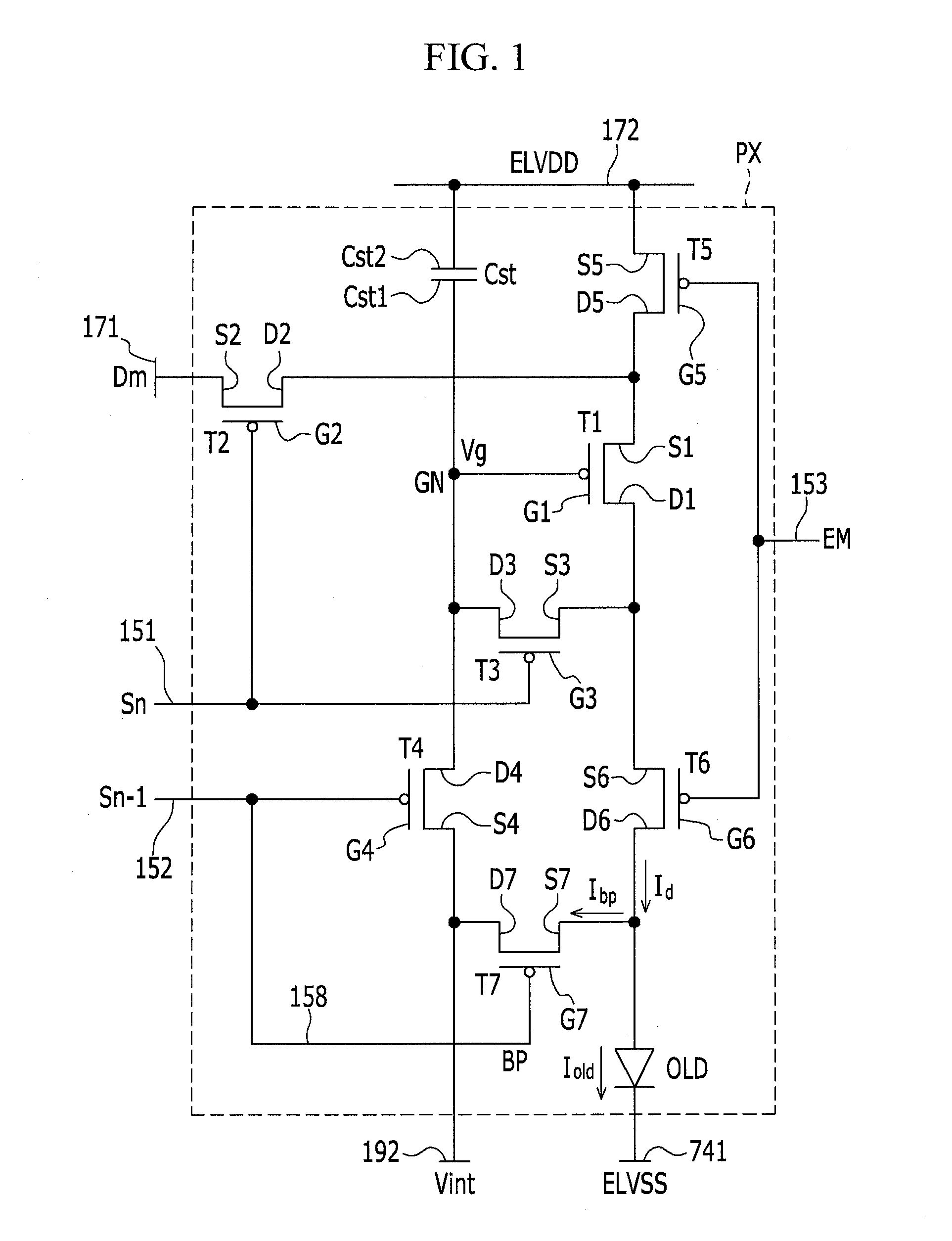
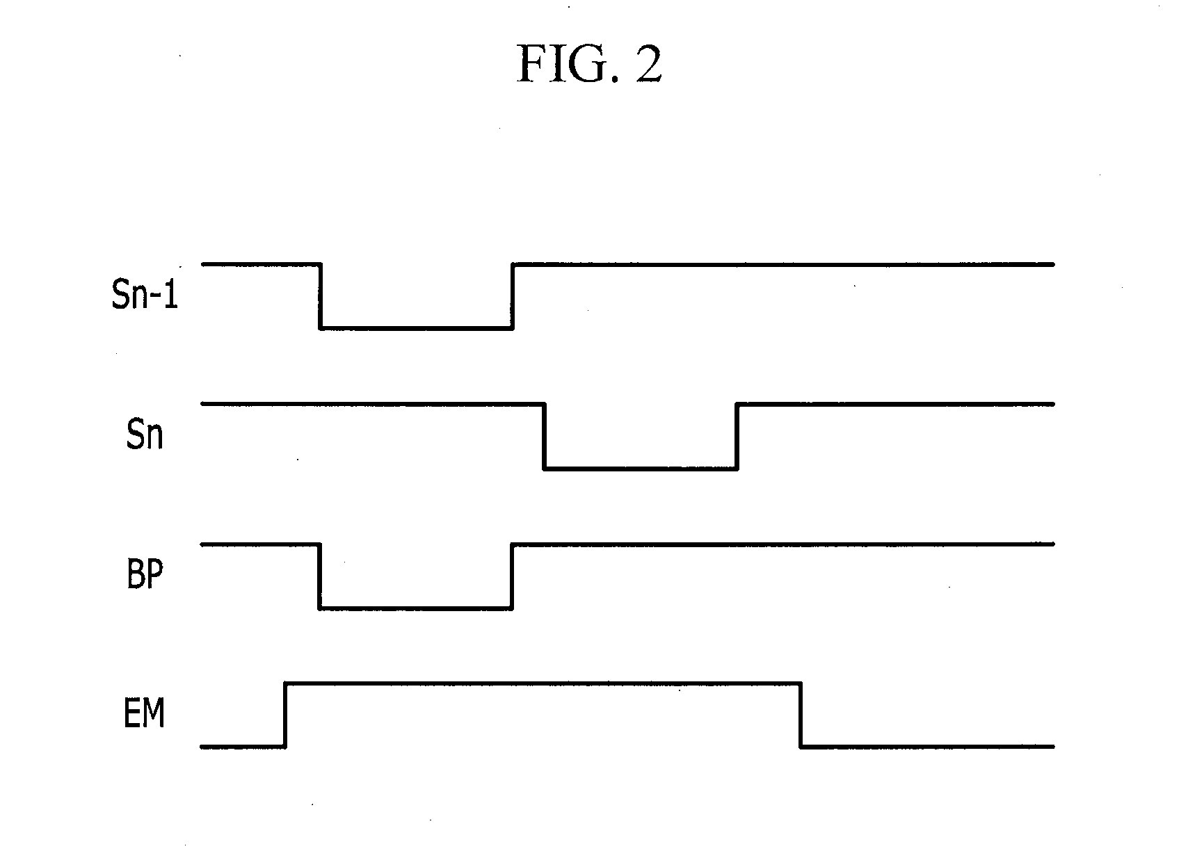
[0045]The present disclosure will be described more fully hereinafter with reference to the accompanying drawings, in which exemplary embodiments of the disclosure are shown. As those skilled in the art would realize, the described embodiments may be modified in various different ways, all without departing from the spirit or scope of the present disclosure.

[0046]The drawings and description are to be regarded as illustrative in nature and not restrictive. Like reference numerals designate like elements throughout the specification.

[0047]Further, because sizes and thicknesses of constituent members and / or layers shown in the accompanying drawings may be arbitrarily shown for better understanding and ease of description, the present disclosure is not limited thereto. In the drawings, the thickness of layers, films, panels, regions, etc., may be exaggerated for clarity.

[0048]It will be understood that when an element or layer is referred to as being “on”, “connected to”, or “coupled t...


PUM


Abstract

An OLED display according to an exemplary embodiment of the present disclosure includes: a substrate; a scan line on the substrate and configured to transmit a scan signal; a data line crossing the scan line and configured to transmit a data voltage; a driving voltage line crossing the scan line and configured to transmit a driving voltage, a portion of the driving voltage line being a second storage electrode; a switching transistor connected to the scan line and the data line; a driving transistor connected to the switching transistor and including a driving gate electrode; a driving connecting member connected to the driving gate electrode; a first storage electrode, the second storage electrode overlapping the first storage electrode; a shielding member connected to the second storage electrode and between the driving connecting member and the data line; and an organic light emitting diode connected to the driving transistor.

Description

CROSS-REFERENCE TO RELATED APPLICATION[0001]This application claims priority to and the benefit of Korean Patent Application No. 10-2015-0009415, filed in the Korean Intellectual Property Office on Jan. 20, 2015, the content of which is incorporated herein in its entirety by reference.BACKGROUND[0002]1. Field[0003]Aspects of embodiments of the present disclosure relate an organic light emitting diode display.[0004]2. Description of the Related Art[0005]An organic light emitting diode display includes two electrodes and an organic light emitting layer positioned therebetween. Electrons injected from a cathode, that is, an electrode, and holes injected from an anode, that is, another electrode, are combined with (e.g., bonded to) each other in the organic light emitting layer to form excitons. Light is emitted when the excitons discharge energy.[0006]The organic light emitting diode display includes a plurality of pixels, each including an organic light emitting diode include the cath...

Claims


Application Information

Patent Timeline
IPC IPC(8): G09G3/32G09G3/20H01L27/32
CPCG09G3/3275H01L27/3244G09G2300/043G09G2320/0209G09G2300/0426G09G3/2092H01L27/1222H01L27/1225H01L27/124H01L27/1255G09G2300/0819G09G2300/0842G09G2300/0861G09G2320/0238G09G3/3233H10K59/1216H10K59/126H10K59/131
Inventor LEE, DONG SUNKIM, DONG-HWILEE, JAE-SIC
Owner SAMSUNG DISPLAY CO LTD
Why Eureka
Try Eureka