Electronic package

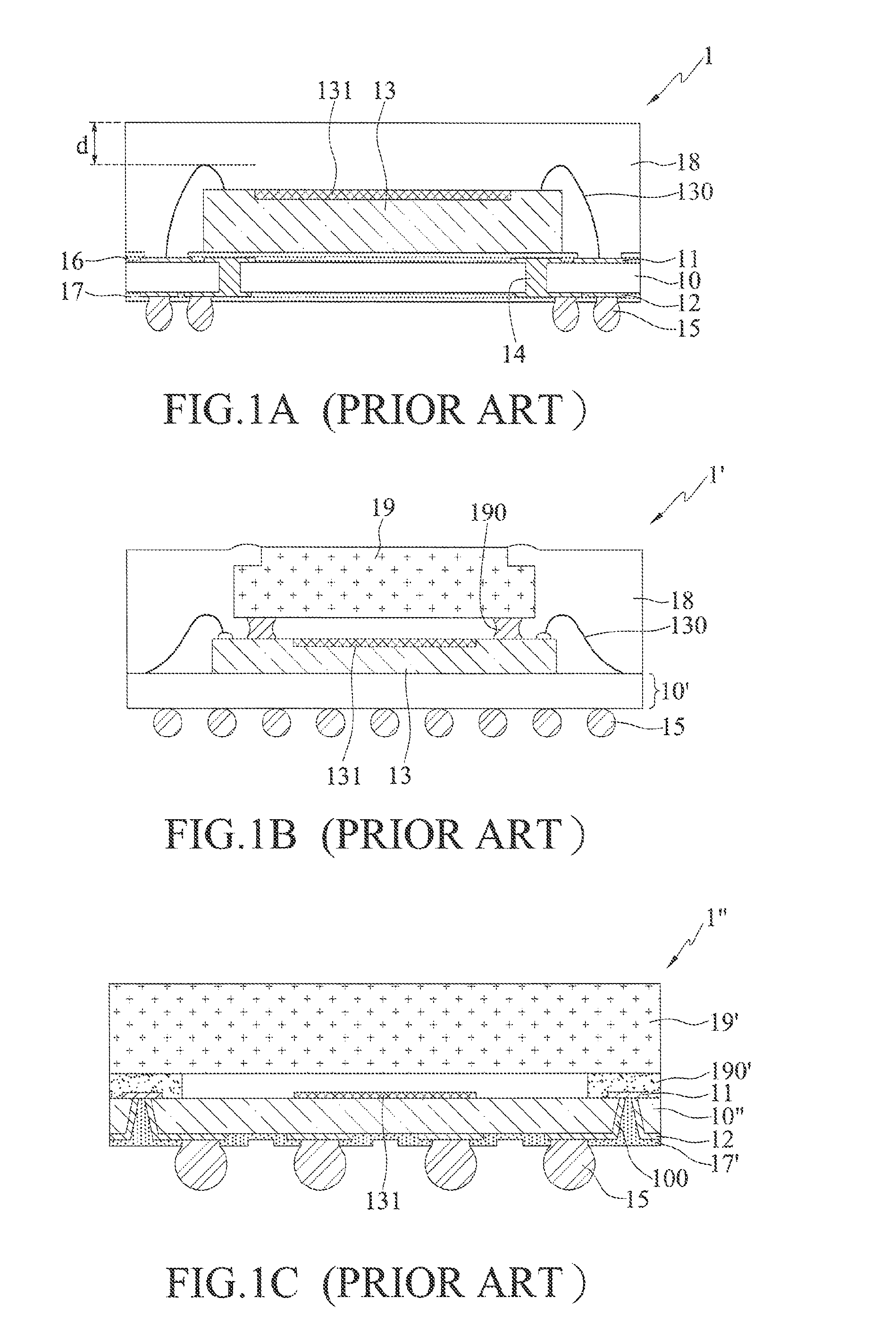
a technology of electronic packaging and encapsulant, which is applied in the direction of electrical apparatus contruction details, printed circuit non-printed electric components association, and semiconductor/solid-state device details, etc. it can solve the problems of difficult control of the thickness of the encapsulant b>18/b>, inability to achieve the thinning of the wire-bonding type package structure b>1/b>, and difficulty in achieving the thinning of the cob typ

Active Publication Date: 2016-07-21
PHOENIX PIONEER TECH
View PDF3 Cites 21 Cited by
  • Summary
  • Abstract
  • Description
  • Claims
  • Application Information

AI Technical Summary

Benefits of technology

[0034]By embedding the electronic element in the insulating layer and electrically connecting the first circuit layer to the electronic element, the present disclosure does not need to consider the wire loo...

Problems solved by technology

As such, the thickness of the encapsulant 18 is difficult to control and thinning of the wire-bonding type package structure 1 cannot be achieved.
However, since the electronic element 13 is attached to the substrate 10′ and the transparent element 19 is disposed on the electronic element 13 thro...

Method used


Image

  • Electronic package
  • Electronic package
  • Electronic package

Examples


first embodiment

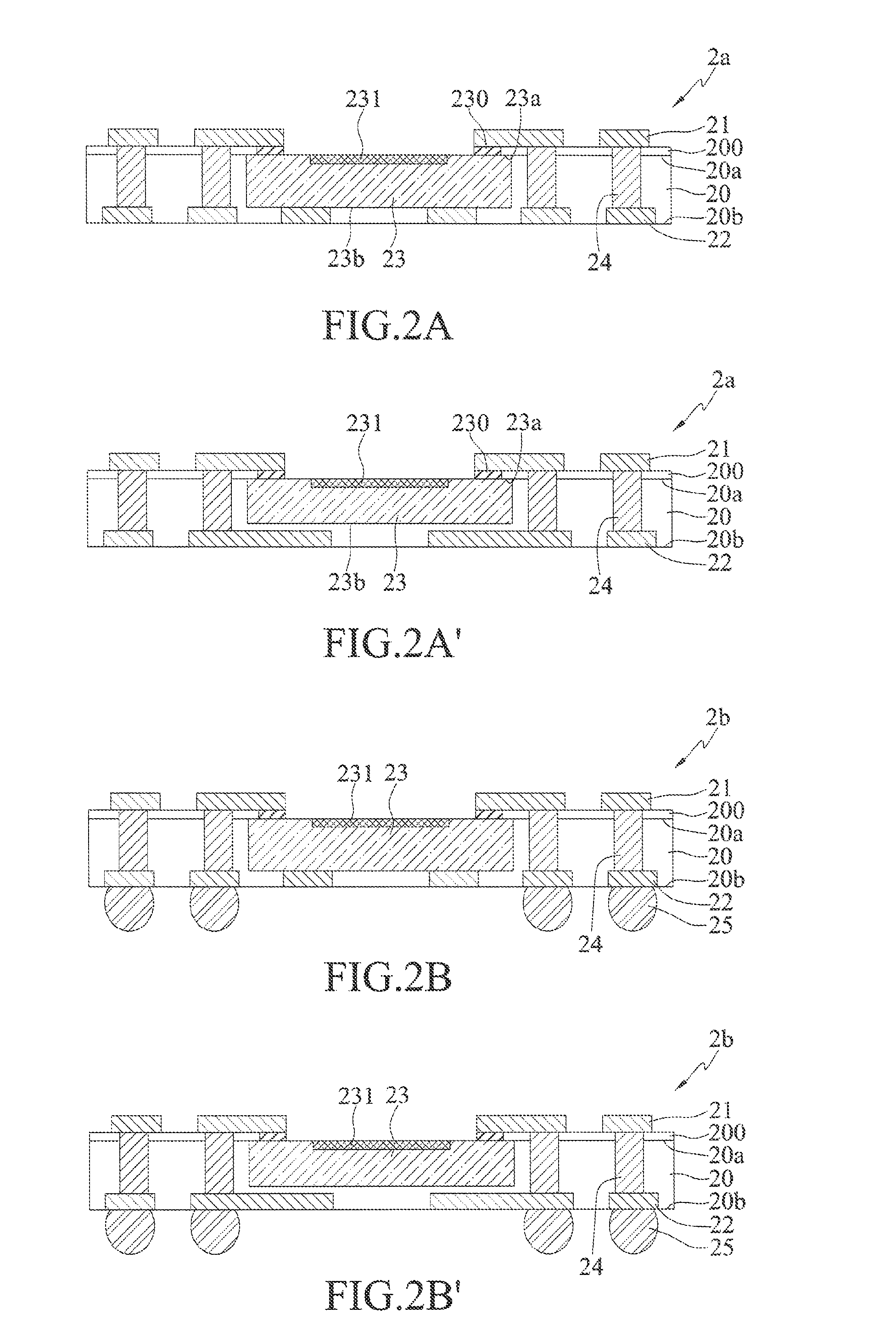
[0044]FIGS. 2A to 2E are schematic cross-sectional views of electronic packages 2a to 2e according to the present disclosure. The electronic packages 2a to 2e are applicable in, for example, fingerprint identifiers and image sensors.

[0045]Referring to FIG. 2A, the electronic package 2a has: a first insulating layer 20 having opposite first and second surfaces 20a, 20b; an electronic element 23 embedded in the first insulating layer 20; a plurality of conductive posts 24 formed in the first insulating layer 20; and a first circuit layer 21 and a second circuit layer 22 formed on the first and second surfaces 20a, 20b of the first insulating layer 20, respectively.

[0046]In the present embodiment, the first insulating layer 20 is made of a molding compound, or a dielectric material such as an epoxy resin, polyimide or other photosensitive or non-photosensitive organic resin. According to the practical need, another insulating layer 200 can be formed on the first surface 20a of the firs...

third embodiment

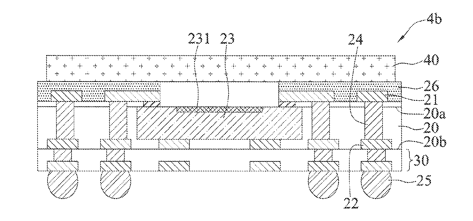
[0071]FIGS. 4A and 4B are schematic cross-sectional views of electronic packages 4a, 4b according to the present disclosure. The present embodiment differs from the above-described embodiments in that the electronic packages 4a, 4b are applicable in camera lenses. In particular, a transparent element 40 is added.

[0072]Referring to FIGS. 4A and 4B, as compared to FIGS. 2D and 3B, the electronic packages 4a, 4b further has a transparent element 40 such as a lens or glass that covers the sensing area 231 of the electronic element 23. For example, the transparent element 40 is attached to the second insulating layer 26. As such, the present disclosure dispenses with the conventional support members so as to reduce the thickness of the overall structure.

[0073]In the electronic package 4a of FIG. 4A, the surface of the second insulating layer 26 is flush with the surface of the first circuit layer 21.

[0074]On the other hand, in the electronic package 4b of FIG. 4B, the first insulating la...


PUM


Abstract

An electronic package is provided, which includes: an insulating layer; an electronic element embedded in the insulating layer and having a sensing area exposed from the insulating layer; and a circuit layer formed on the insulating layer and electrically connected to the electronic element, thereby reducing the thickness of the overall package structure.

Description

[0001]BACKGROUND[0002]1. Technical Field[0003]The present disclosure relates to an electronic package, and more particularly, to a thin-type electronic package.[0004]2. Description of Related Art[0005]Along with the rapid development of electronic industries, electronic products are developed toward the trend of miniaturization and multi-function. Accordingly, various types of packages have been developed.[0006]Generally, electronic elements of sensor elements and camera lenses are packaged to form wire-bonding or COB (Chip on Board) type package structures.[0007]FIG. 1A is a schematic cross-sectional view of a conventional wire-bonding type package structure 1. Referring to FIG. 1A, the conventional wire-bonding type package structure 1 has a substrate 10, an electronic element 13 disposed on the substrate 10, and an encapsulant 18 formed on the substrate 10 and encapsulating the electronic element 13.[0008]A first circuit layer 11 and a second circuit layer 12 are formed on upper ...

Claims


Application Information

Patent Timeline
IPC IPC(8): H05K1/18H05K1/02H05K1/11H05K1/03
CPCH05K1/181H05K1/111H05K1/0298H05K1/0313H01L2924/181H01L23/5389H05K1/185H05K2201/10121H05K2201/10151H01L27/14618H01L2224/48091H01L2224/48227H01L2924/15311H01L2924/16235H01L2224/45144H01L2224/48465H01L24/24H01L24/82H01L2924/16251H01L2924/16195H01L23/10H01L2224/24225H01L2924/16315G06V40/1318H01L2924/00012H01L2924/00014H01L2924/00015H01L2924/00H01L2224/18H05K2201/10H05K3/284
Inventor HU, CHU-CHINHSU, SHIH-PING
Owner PHOENIX PIONEER TECH
Why Eureka
Try Eureka