Memory device with adaptive voltage scaling based on error information

a memory device and error information technology, applied in the field of memory devices with adjustable supply voltage, can solve the problems of data error number, voltage stress of sram devices, consumption of power, etc., and achieve the effect of reducing one or more effects of degradation, reducing operating margins, and reducing operating margins

Active Publication Date: 2016-08-04
QUALCOMM INC
View PDF9 Cites 54 Cited by
  • Summary
  • Abstract
  • Description
  • Claims
  • Application Information

AI Technical Summary

Benefits of technology

[0014]One particular advantage provided by at least one of the disclosed aspects is a method of providing a supply voltage to a memory device that may be adaptively scaled based on performance of the memory device. Adaptively scaling the supply voltage may compensate for degradation to the memory device during the operational life of the memory device. For example, the memory device may be an SRAM, and the reliability of the SRAM may degrade during the operational life of the SRAM due to bias temperature instability (BTI) experienced by the SRAM. Because the supply voltage is adaptively scaled, the supply voltage may initially be provided at a lower voltage level than a “pessimistic” voltage level estimated based on “worst-case” estimates, and the supply voltage may be increased later in the operational life of the memory device to reduce one or more effects of the degradation. By adaptively scaling the voltage, instead of setting the voltage level to the pessimistic estimate, the memory device may operate with reduced operating margins, such as a voltage supply margin. Additionally, by determining target voltage levels for each of multiple operating frequencies, the memory device may operate with reduced operating margins at multiple operating frequencies. Operating with reduced operating margins may provide cost and power savings as compared to memory devices that are not able to dynamically scale the supply voltage. Additionally, operating at lower voltage levels may decrease voltage stress to transistors of the memory device, which may increase the operational life of the memory device.

Problems solved by technology

The worst case scenario may take into account performance and reliability degradations of the SRAM device over time resulting from bias temperature instability (BTI) experienced at cells of the memory device.
However, operating a “strong” (e.g., fast) SRAM device based on the worst case scenario consumes power and may cause voltage stress to transistors of the SRAM device.
Error detection circuitry may be coupled to the array and may determine whether errors exist in data accessed from the array when the array is operated at a first operating frequency.
Adjustment circuitry coupled to the error detection circuitry may determine a number of errors in the data.
If the number of errors satisfies the threshold when the supply voltage is set to the highest test voltage, a failure condition may be generated.
During the operational life of the memory device, the array (e.g., the memory device) may experience degradation due to aging, which may change operation of the array.
For example, the memory device may be an SRAM, and the reliability of the SRAM may degrade during the operational life of the SRAM due to bias temperature instability (BTI) experienced by the SRAM.
Additionally, operating at lower voltage levels may decrease voltage stress to transistors of the memory device, which may increase the operational life of the memory device.

Method used


Image

  • Memory device with adaptive voltage scaling based on error information
  • Memory device with adaptive voltage scaling based on error information
  • Memory device with adaptive voltage scaling based on error information

Examples


Embodiment Construction

[0021]Particular embodiments of the present disclosure are described below with reference to the drawings. In the description, common features are designated by common reference numbers.

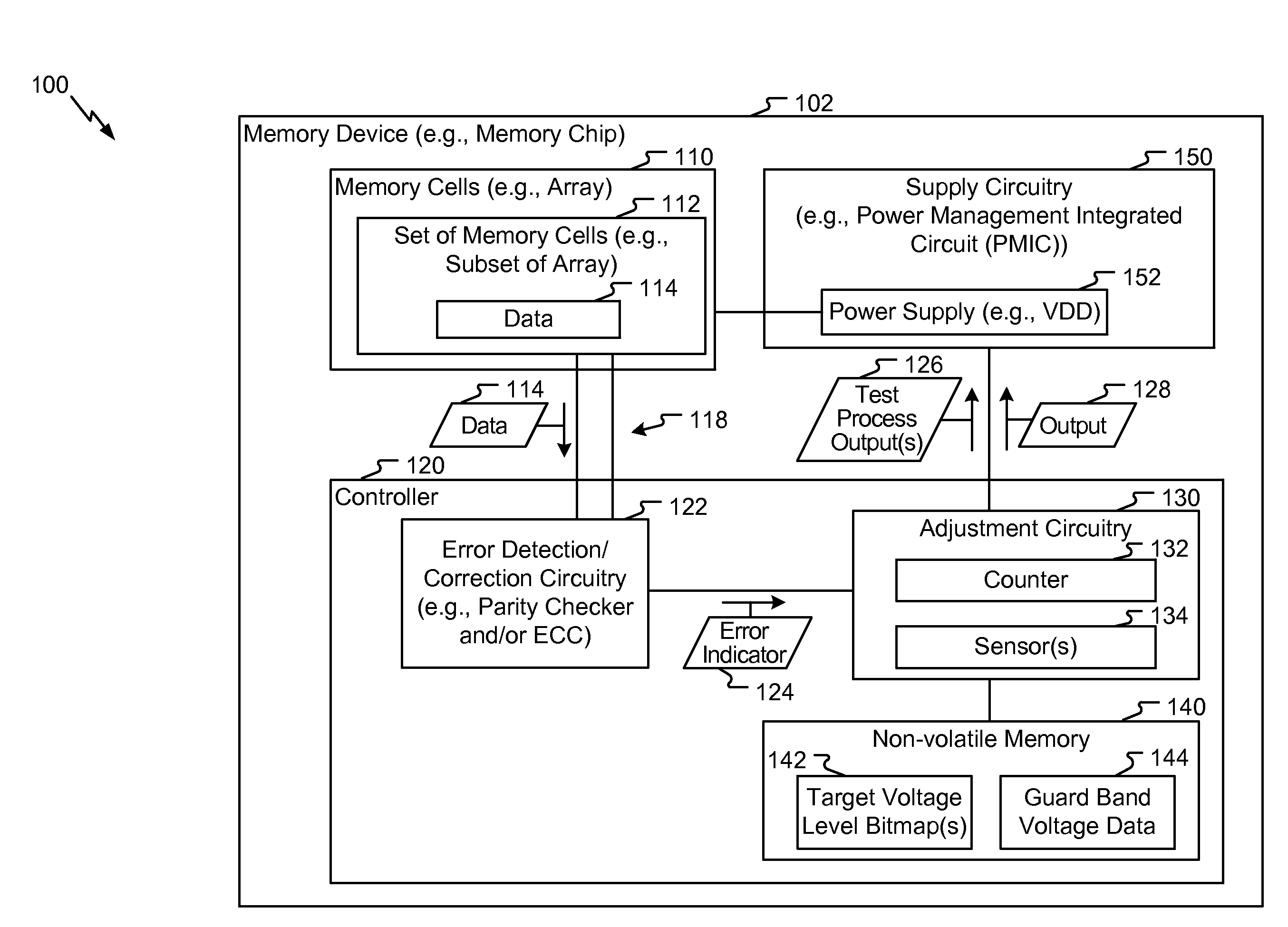
[0022]Referring to FIG. 1, a particular illustrative embodiment of a system 100 configured to determine, for multiple operating frequencies of an array of memory cells, target voltage levels based on errors detected in data stored at the array and to adjust a supply voltage (VDD) provided to the array is disclosed. The system 100 includes a memory device 102, such as a memory chip (e.g., a memory die). The memory device 102 may include a memory array 110, a controller 120, and supply circuitry 150. In a particular embodiment, the memory array 110 is a static random access memory (SRAM) array. In other embodiments, the memory array 110 is another type of memory array.

[0023]The memory array 110 may include a plurality of memory cells. A set of memory cells 112 of the memory array 110 (e.g., a subset of...


PUM


Abstract

A method of operation of a memory device includes, for each operating frequency of multiple operating frequencies, determining a target voltage level of a supply voltage. For example, a first target voltage level for a first operating frequency of the multiple operating frequencies is determined. The method includes accessing first data from the memory device while the memory device is operating at the first operating frequency and is powered by the supply voltage having a first voltage level. The method includes determining a first number of errors associated with the first data. The method further includes, in response to the first number of errors satisfying a threshold, adjusting the supply voltage to a second voltage level that is greater than the first voltage level.

Description

I. FIELD[0001]The present disclosure is generally related to a memory device with an adjustable supply voltage.II. DESCRIPTION OF RELATED ART[0002]Advances in technology have resulted in smaller and more powerful computing devices.[0003]For example, a variety of portable personal computing devices, including wireless telephones such as mobile and smart phones, tablets and laptop computers are small, lightweight, and easily carried by users. These devices can communicate voice and data packets over wireless networks. Further, many such devices incorporate additional functionality such as a digital still camera, a digital video camera, a digital recorder, and an audio file player. Also, such devices can process executable instructions, including software applications, such as a web browser application, that can be used to access the Internet. As such, these devices can include significant computing and networking capabilities.[0004]A computing device, such as a wireless computing devi...

Claims


Application Information

Patent Timeline
Patent Type & Authority Applications(United States)
IPC IPC(8): G11C11/417G06F11/07
CPCG11C11/417G06F11/0793G06F11/076G06F11/073G11C5/14G11C5/147G11C7/1045G11C7/22G11C29/021G11C29/028G11C2207/2254
Inventor WANG, ZHONGZEMOJUMDER, NILADRI NARAYANLIU, JONATHANYEAP, CHOH FEI
Owner QUALCOMM INC
Why Eureka
Try Eureka