Solder material and electronic component
- Summary
- Abstract
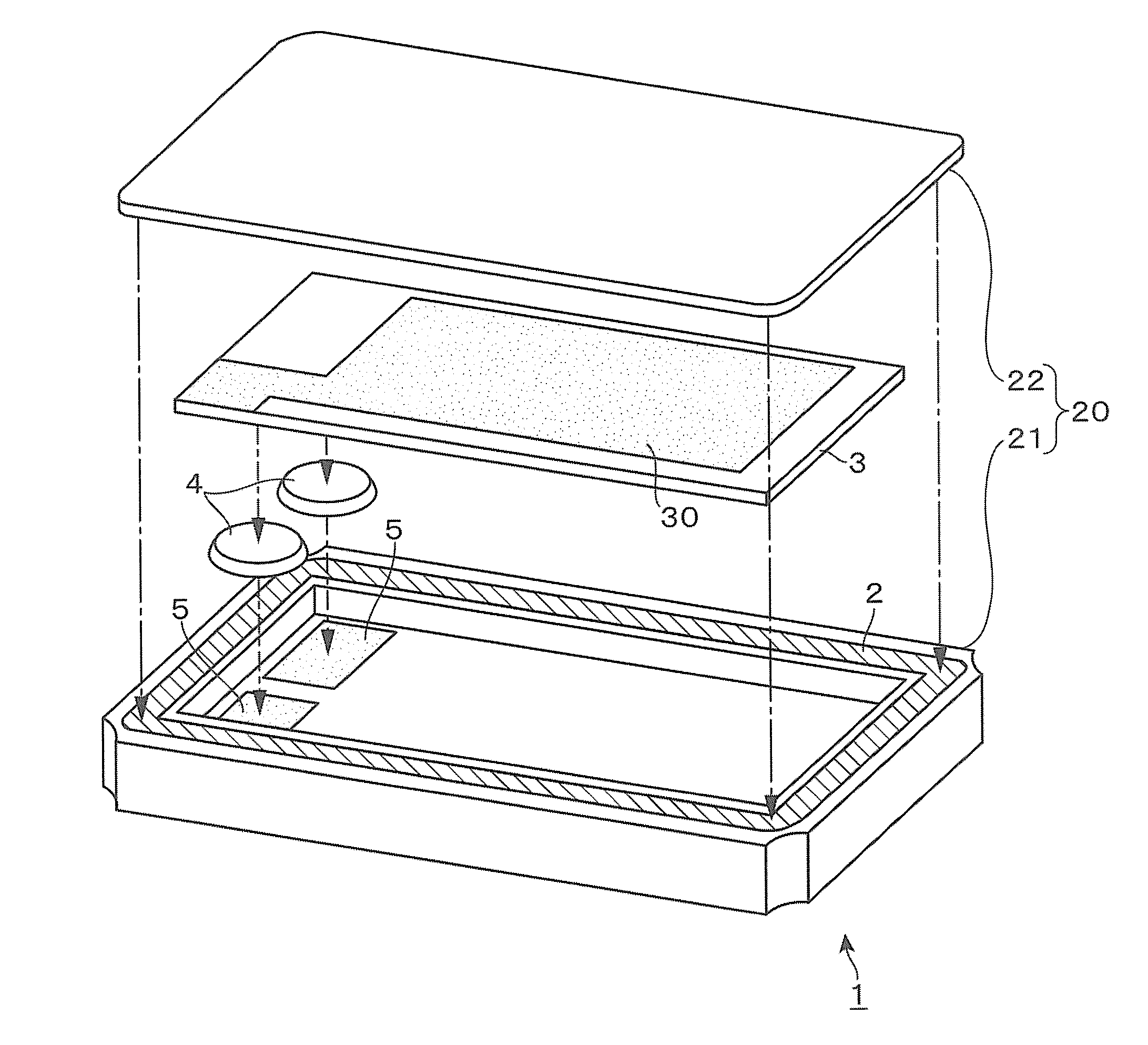
- Description
- Claims
- Application Information
AI Technical Summary
Benefits of technology
Problems solved by technology
Method used
Image

Examples
working example 1
[0051]The composition ratio was set such that solder material contains 38.0 mass % of Sn, 36.0 mass % of Sb, 15.0 mass % of Ag, 5.0 mass % of Cu, and 6.0 mass % of In. This solder material was manufactured by a known manufacturing method of a solder material described in the embodiment disclosed here.
working examples 2 to 27
[0052]These solder materials were manufactured similar to Working Example 1, except that the composition ratios of the solder materials were set as indicated in Table 1 described later.
working example 1-2
[0076]Working Example 1-2 employed a solder material that was obtained by replacing 0.01 mass % of the mixed solder material of Working Example 1 by 0.005 mass % of Si and 0.005 mass % of Ti.
PUM
| Property | Measurement | Unit |
|---|---|---|
| Temperature | aaaaa | aaaaa |
| Temperature | aaaaa | aaaaa |
| Temperature | aaaaa | aaaaa |
Abstract
Description
Claims
Application Information
 - R&D Engineer
- R&D Manager
- IP Professional
- Industry Leading Data Capabilities
- Powerful AI technology
- Patent DNA Extraction
Browse by: Latest US Patents, China's latest patents, Technical Efficacy Thesaurus, Application Domain, Technology Topic.
© 2024 PatSnap. All rights reserved.Legal|Privacy policy|Modern Slavery Act Transparency Statement|Sitemap