Device for radiofrequency (RF) transmission with an integrated electromagnetic wave reflector

a radiofrequency (rf) and reflector technology, applied in the direction of electrical equipment, basic electric elements, antennas, etc., can solve the problems of mediocre positioning precision, complicated form, and limited routing line resolution resolution techniques

Active Publication Date: 2016-08-11
COMMISSARIAT A LENERGIE ATOMIQUE ET AUX ENERGIES ALTERNATIVES
View PDF1 Cites 40 Cited by
  • Summary
  • Abstract
  • Description
  • Claims
  • Application Information

AI Technical Summary

Problems solved by technology

These devices nevertheless have several drawbacks:they are complex to form because they bring into play a large number of layers.
They are especially suited to be produced via PCB (printed circuit board) manufacturing techniques, but said techniques are limited in terms of the resolutions of routing lines and vertical interconnections which can be obtained, which is highly penalizing for high frequency transmissions (for example above 60 GHz).
Furthermore, the positioning precisions which can be obtained are also mediocre (generally above 500 μm),they are bulky, especially in terms of thickness because the cavities of the antennas are superimposed on the cavity of the chip,they only enable the use of a single frequency band for which the antennas are optimized,the rear face of the chip is not or is very little in contact with the packaging which is itself made of organic material which is a poor heat conductor.
However, it necessitates having a reflector arranged on the PCB transfer substrate, which limits the routing density which can be obtained on the PCB.
Furthermore, this type of structure implies eliminating the connection beads under the antennas, which considerably reduces the mechanical reliability of the structure.
Finally, the RFIC chip is immersed in a material that conducts heat very poorly, which considerably adversely affects heat dissipation.
Despite a possible advantage in terms of resolution of patterns which can be obtained, this solution also suffers from a certain number of drawbacks:a reflective plane is necessarily arranged on the PCB, which implies design constraints and losses of space for the routing;connection beads are absent at the reflector, which reduces the reliability of the beading and thus the mechanical integrity of the assembly;the height of the beads has a very important impact on the structure obtained after assembly, and thus also on the properties of the antennas;a single height is possible at the antennas, which implies a single possible transmission frequency band for the device;the heat dissipation of the RFIC chip is insufficient.
Generally speaking, these different RF transmission devices suffer from an important bulk due to the cavities or to the distance that has to be maintained between the reflective planes and the antennas.

Method used


Image

  • Device for radiofrequency (RF) transmission with an integrated electromagnetic wave reflector
  • Device for radiofrequency (RF) transmission with an integrated electromagnetic wave reflector
  • Device for radiofrequency (RF) transmission with an integrated electromagnetic wave reflector

Examples


first embodiment

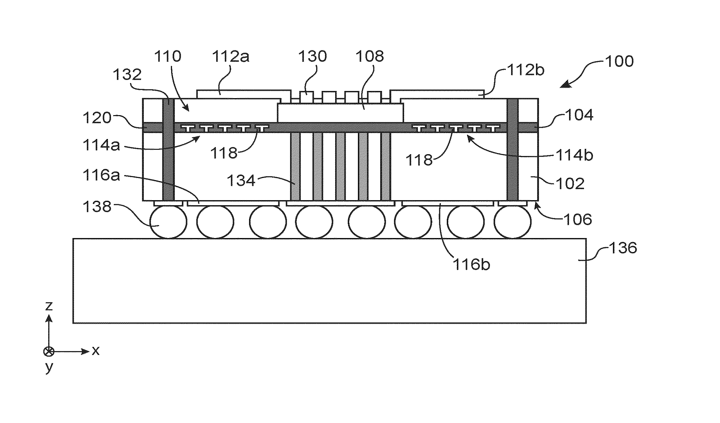
[0096]FIGS. 1 and 4 show a RF transmission device ;

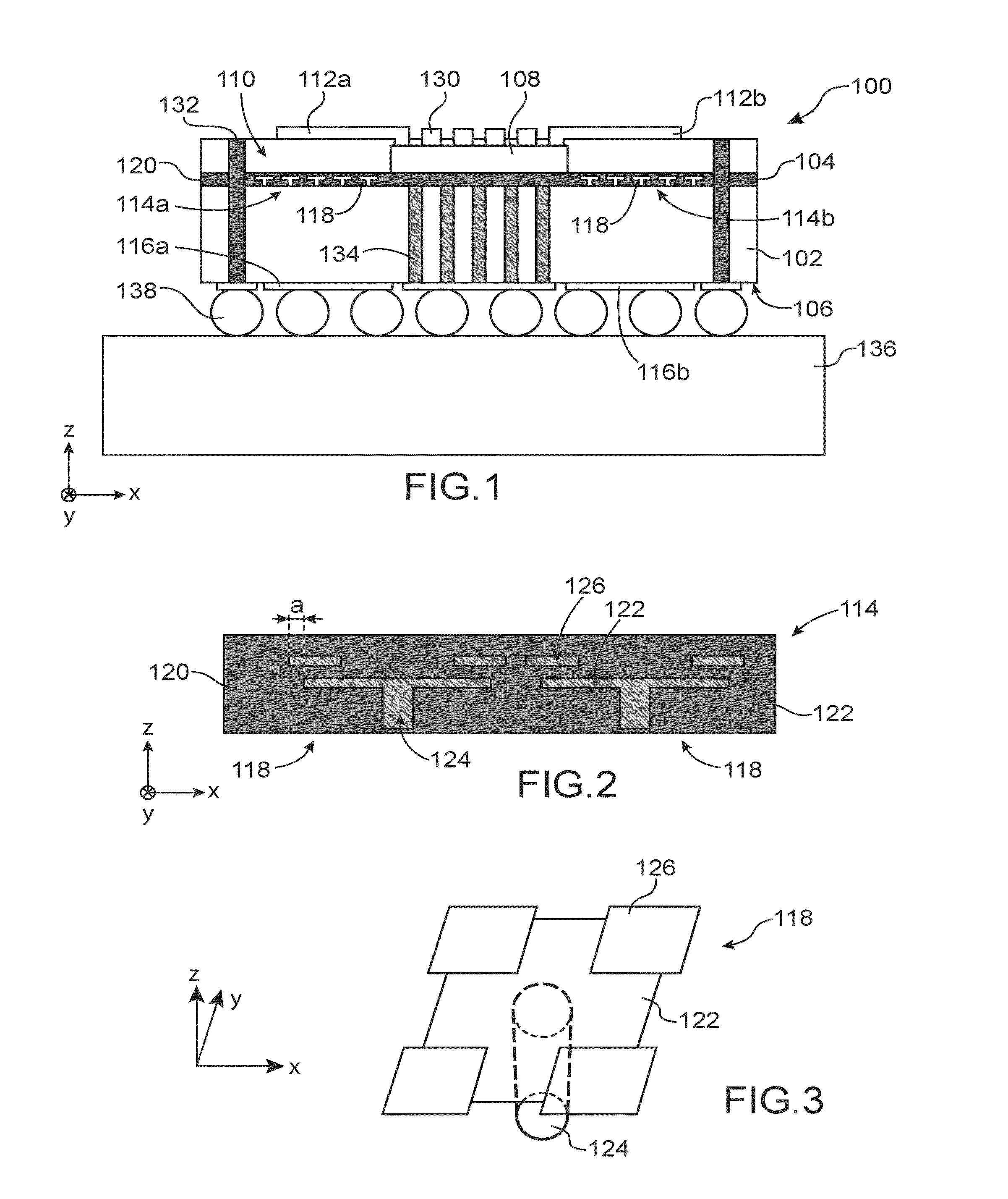
[0097]FIGS. 2 and 3 show an example of embodiment of electrically conducting elements of a high impedance surface of a RF transmission device;

second embodiment

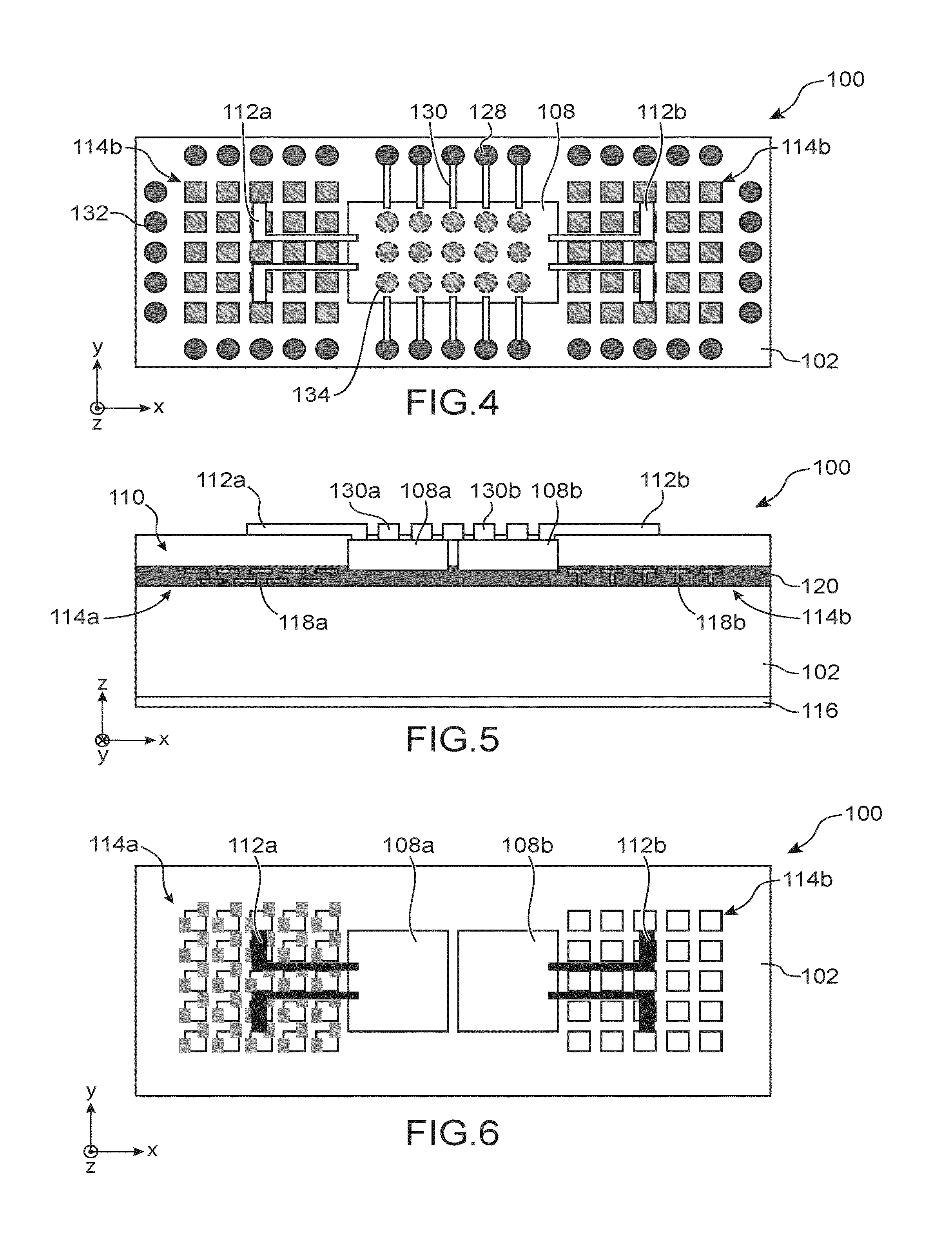
[0098]FIGS. 5 and 6 show a part of a RE transmission device ;

[0099]FIG. 7 shows a part of a RF transmission device according to a variant of the first embodiment.

[0100]Identical, similar or equivalent parts of the different figures described hereafter bear the same numerical references so as to make it easier to go from one figure to the next.

[0101]The different parts shown in the figures are not necessarily according to a uniform scale, in order to make the figures more legible.

[0102]The different possibilities (variants and embodiments) must be understood as not being mutually exclusive and can be combined together.


PUM


Abstract

RF transmission device including at least:
    • a substrate comprising first and second faces opposite to each other;
    • a first RF transmission electronic circuit arranged on and/or in the substrate;
    • a first antenna arranged on the side of the first face of the substrate, spaced apart from the first face of the substrate and electrically connected to the first RF transmission electronic circuit;
    • a first electromagnetic wave reflector coupled to the first antenna and including:
      • a first high impedance surface comprising at least several first electrically conducting elements forming a first periodic structure and arranged on the first face of the substrate opposite the first antenna;
      • a first electrically conducting ground plane arranged at least partially opposite the first antenna.

Description

TECHNICAL FIELD AND PRIOR ART[0001]The invention relates to a radiofrequency (RF) transmission device comprising at least one RF transmission electronic circuit coupled to at least one integrated electromagnetic wave reflector enabling the formation of the device with low thickness, high gain and good efficiency. The invention may apply notably to the field of RF transmission for frequencies which can range from around 1 GHz to around 300 GHz, and advantageously between around 30 GHz and 250 GHz.[0002]In the field of RF transmission devices, the integration and the packaging of RF components, also called RFIC chips or RF transmission electronic circuits, and their antennas are becoming more and more important in terms of bulk, electrical performances, heat dissipation and cost. In particular, the connections of RF electronic components to antennas become particularly critical in terms of losses (the interconnections and the antennas generally account for around half of the overall p...

Claims


Application Information

Patent Timeline
Patent Type & Authority Applications(United States)
IPC IPC(8): H01L23/66H01L23/498H01L21/48H01L25/065H01L25/00H01L23/552H01L23/367
CPCH01L21/4846H01Q9/26H01L25/50H01L25/0655H01L2223/6677H01L23/552H01L23/49833H01L23/49827H01L23/367H01L23/66H01L23/3677H01L23/498H01L23/49816H01L23/5389H01L24/19H01P1/20H01Q15/008H01L2224/04105H01L2224/73267H01L2924/15313H01L2223/6616H01Q1/2283H01Q21/28
Inventor LAMY, YANNDUSSOPT, LAURENTEL BOUAYADI, OSSAMAMOKNACHE, AMAZIR
Owner COMMISSARIAT A LENERGIE ATOMIQUE ET AUX ENERGIES ALTERNATIVES
Why Eureka
Try Eureka