
Manufacturing method and structure of thin film transistor backplane

a manufacturing method and backplane technology, applied in the field of flat panel display, can solve the problems of more considerable accumulated yield problem, less yield of production, and longer process time, and achieve the effect of reducing the number of manufacturing steps, and reducing the cost of production

Active Publication Date: 2016-08-18
SHENZHEN CHINA STAR OPTOELECTRONICS TECH CO LTD
View PDF0 Cites 6 Cited by
  • Summary
  • Abstract
  • Description
  • Claims
  • Application Information

AI Technical Summary

Benefits of technology

The present invention provides a method for manufacturing a thin film transistor backplane using a simplified process that eliminates the need for multiple photolithographic steps. This reduces the production time and increases efficiency, resulting in a higher yield of production. Additionally, the invention structures a thin film transistor backplane that eliminates issues of contact resistance and occupies less space, promoting the efficiency of OLED display technology.

Problems solved by technology

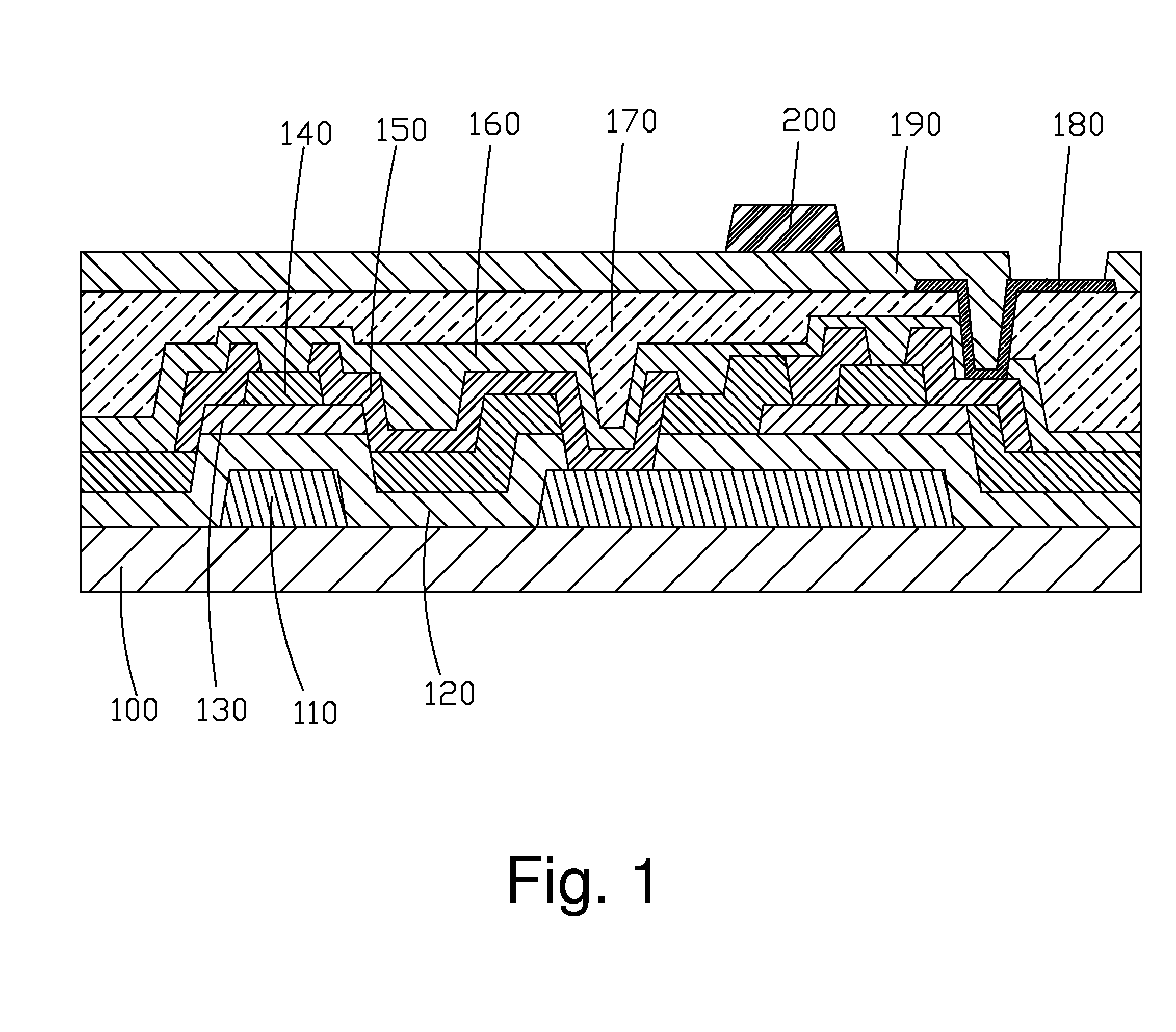
Certain disadvantages exist in the manufacture method of the thin film transistor backplane in the AM-OLED.
Mainly, it can be understood that the formation of each layer requires one photolithographic process (Every photolithographic process comprises manufacture processes of thin film, photo, etching, stripping and etc.) The more the photolithographic process is required, the process time takes longer and the yield of the production becomes lower; with more numbers of processes, the more considerable accumulated yield problem is.

Method used


Image

  • Manufacturing method and structure of thin film transistor backplane
  • Manufacturing method and structure of thin film transistor backplane
  • Manufacturing method and structure of thin film transistor backplane

Examples


first embodiment

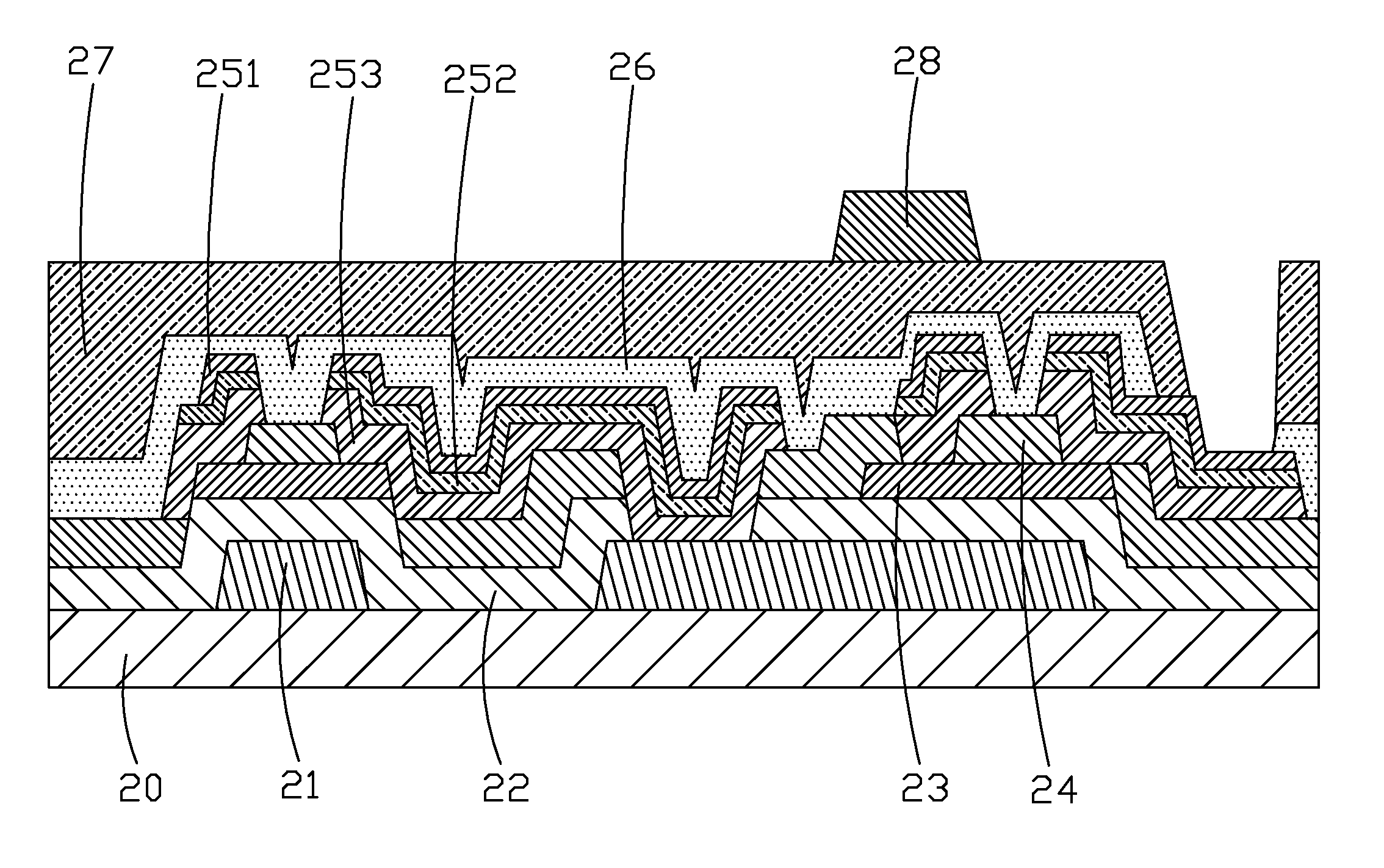
[0047]The step 1 can be achieved by present skills. In step 1 of the first embodiment, the substrate 20 is a transparent substrate. Preferably, the substrate 20 is a glass substrate. On the substrate 20, the gate 21 on the substrate 20, the insulation layer 22 on the gate 21, the semiconducting layer 23 on the insulation layer 22 and an etching stopper layer 24 on the semiconducting layer 23 are formed. The gate 21, the insulation layer 22, the semiconducting layer 23 and the etching stopper layer 24 are sequentially formed on the substrate 20 with respective photolithographic process.

[0048]The semiconducting layer 23 can be an oxide semiconducting layer, such as an indium gallium zinc oxide semiconducting layer (IGZO), or an amorphous silicon (a-Si) semiconducting layer, a polysilicon (p-Si) semiconducting layer or an organic semiconducting layer.

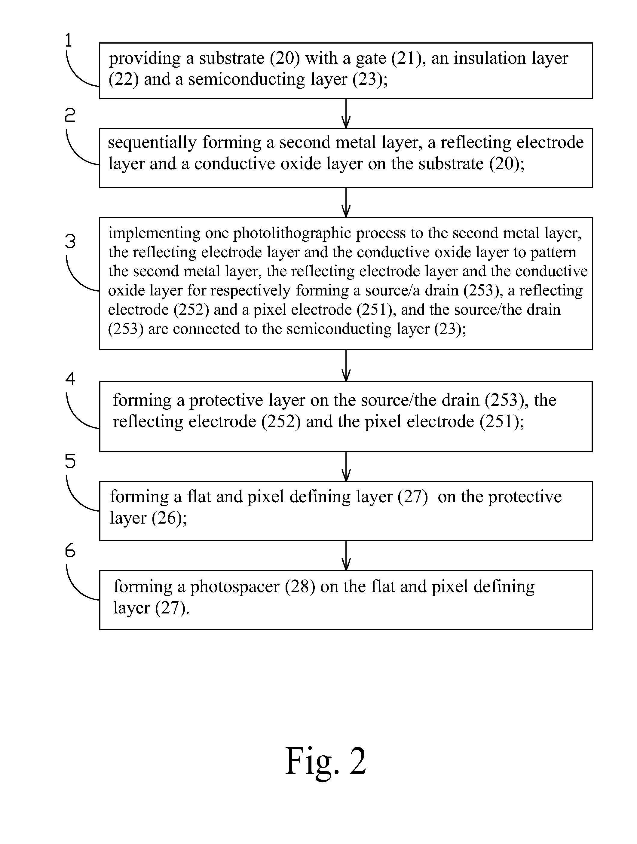
[0049]step 2, sequentially forming a second metal layer, a reflecting electrode layer and a conductive oxide layer on the substrate 20;

[0...

second embodiment

[0060]In step 1 of the second embodiment, the substrate 20′ is a transparent substrate. Preferably, the substrate 20′ is a glass substrate. On the substrate 20′, the gate 21′ on the substrate 20′, the insulation layer 22′ on the gate 21′ and the semiconducting layer 23′ on the insulation layer 22′ are formed. The gate 21′, the insulation layer 22′ and the semiconducting layer 23′ are sequentially formed on the substrate 20′ with respective photolithographic process.

[0061]The semiconducting layer 23′ can be an oxide semiconducting layer, such as an indium gallium zinc oxide semiconducting layer (IGZO), or an amorphous silicon (a-Si) semiconducting layer, a polysilicon (p-Si) semiconducting layer or an organic semiconducting layer.

[0062]Other steps are the same as those described in the first embodiment. The repeated explanation is omitted here.

[0063]Please refer to FIG. 10 and FIG. 11, which are diagrams of the third embodiment of the manufacture method of the thin film transistor ba...

third embodiment

[0065]In step 1 of the third embodiment, the substrate 20″ is a transparent substrate. Preferably, the substrate 20″ is a glass substrate. On the substrate 20″, a buffer layer 35 on the substrate 20″, a semiconducting layer 23″ on the buffer layer 35, an insulation layer 22″ on the semiconducting layer 23″, a gate 21″ on the insulation layer 22″ and a second insulation layer 37 on the gate 21″ are formed. The buffer layer 35, the semiconducting layer 23″, the insulation layer 22″, the gate 21″ and the second insulation layer 37 are sequentially formed on the substrate 20″.

[0066]The semiconducting layer 23″ can be an oxide semiconducting layer, such as an indium gallium zinc oxide semiconducting layer (IGZO), or an amorphous silicon (a-Si) semiconducting layer, a polysilicon (p-Si) semiconducting layer or an organic semiconducting layer.

[0067]Other steps are the same as those described in the first embodiment. The repeated explanation is omitted here.

[0068]The present invention furth...


PUM

PropertyMeasurementUnit
semiconductingaaaaaaaaaa
conductiveaaaaaaaaaa
transparentaaaaaaaaaa

Abstract

The present invention provides a manufacture method of a thin film transistor backplane, comprising steps of: providing a substrate (20) with a gate (21), an insulation layer (22) and a semiconducting layer (23); sequentially forming a second metal layer, a reflecting electrode layer and a conductive oxide layer on the substrate (20); implementing one photolithographic process to the second metal layer, the reflecting electrode layer and the conductive oxide layer to pattern the second metal layer, the reflecting electrode layer and the conductive oxide layer for respectively forming a source / a drain (253), a reflecting electrode (252) and a pixel electrode (251), and the source / the drain (253) are connected to the semiconducting layer (23; forming a protective layer on the source / the drain (253), the reflecting electrode (252) and the pixel electrode (251; forming a flat and pixel defining layer (27) on the protective layer (26); forming a photospacer (28) on the flat and pixel defining layer (27).

Description

FIELD OF THE INVENTION[0001]The present invention relates to a skill field of a flat panel display, and more particularly to a manufacture method and a structure of a thin film transistor backplane.BACKGROUND OF THE INVENTION[0002]A flat panel display possesses advantages of being ultra thin, power saved and radiation free. It has been widely utilized. A present flat panel display mainly comprises a LCD (Liquid Crystal Display) or an OLED (Organic Light Emitting Display).[0003]An OLED possesses many outstanding properties of self-illumination, no requirement of backlight, high contrast, ultra-thin, wide view angle, fast response, applicability of flexible panel, wide range of working temperature, simpler structure and process. The OLED is considered as next generation flat panel display technology.[0004]Generally, OLED comprises a substrate, ITO (Indium Tin Oxide) transparent anode located on the substrate, a Hole Injection Layer (HIL) located on the ITO transparent anode, a Hole Tr...

Claims


Application Information

Patent Timeline
Patent Type & Authority Applications(United States)
IPC IPC(8): H01L27/32H01L51/00H01L27/12H01L51/56
CPCH01L21/77H01L27/12H01L27/1214H01L27/1225H01L2227/323H01L51/0023H01L51/5206H01L51/56H01L27/3262H01L27/124H01L27/1288H10K71/621H10K71/00H10K59/80516H10K59/8051H10K59/1201H10K59/1213H10K50/81
Inventor LI, WENHUIZHANG, HEJINGSHI, LONGQIANG
Owner SHENZHEN CHINA STAR OPTOELECTRONICS TECH CO LTD
Learn More