

Substrate pretreatment method and apparatus
a pretreatment method and substrate technology, applied in the direction of electrical equipment, conveyor parts, semiconductor devices, etc., can solve the problems of affecting the degree of drying of the substrate is very critical, and the damage to the oled device after the device, so as to save the baking time in the loading chamber, improve the performance and life of the oled device, and reduce the tact time
- Summary
- Abstract
- Description
- Claims
- Application Information
AI Technical Summary
Benefits of technology
Problems solved by technology
Method used
Image

Examples
Embodiment Construction
[0034]In order to more specifically describe the technical means and the effects of the present invention, the best embodiments and drawings are described in detail as follows.
[0035]Please refer to FIGS. 1-3. The present invention provides a substrate pretreatment method, which includes the steps as follows:
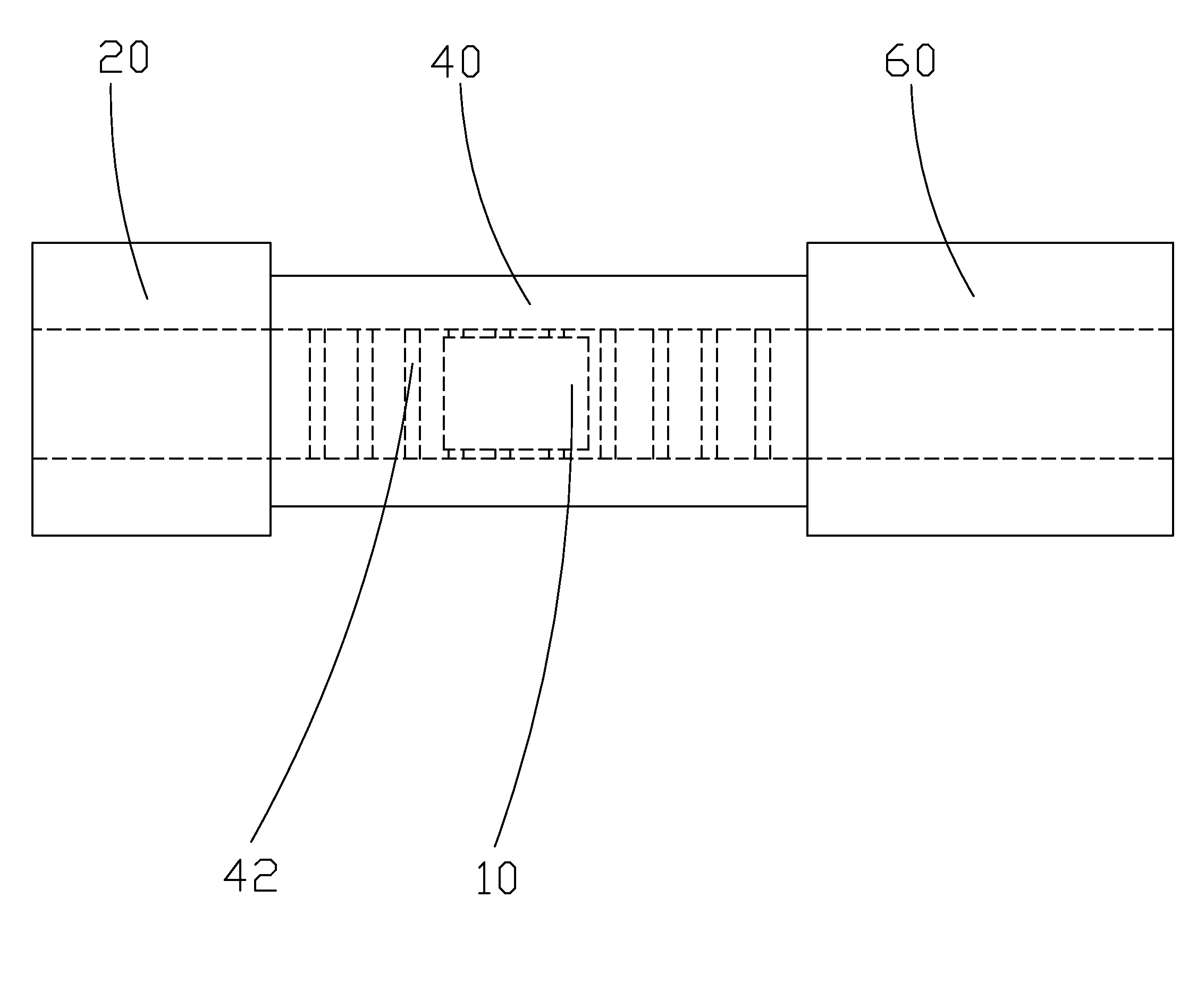
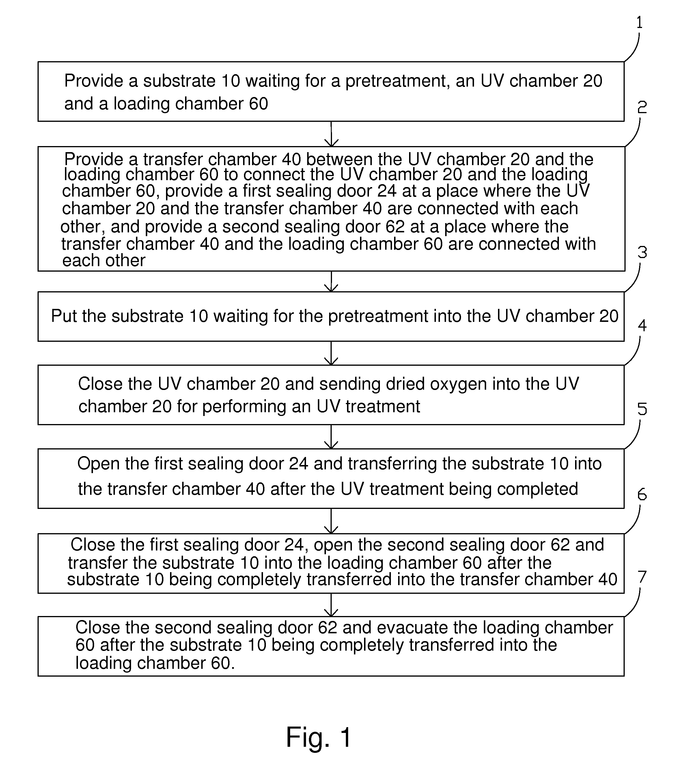
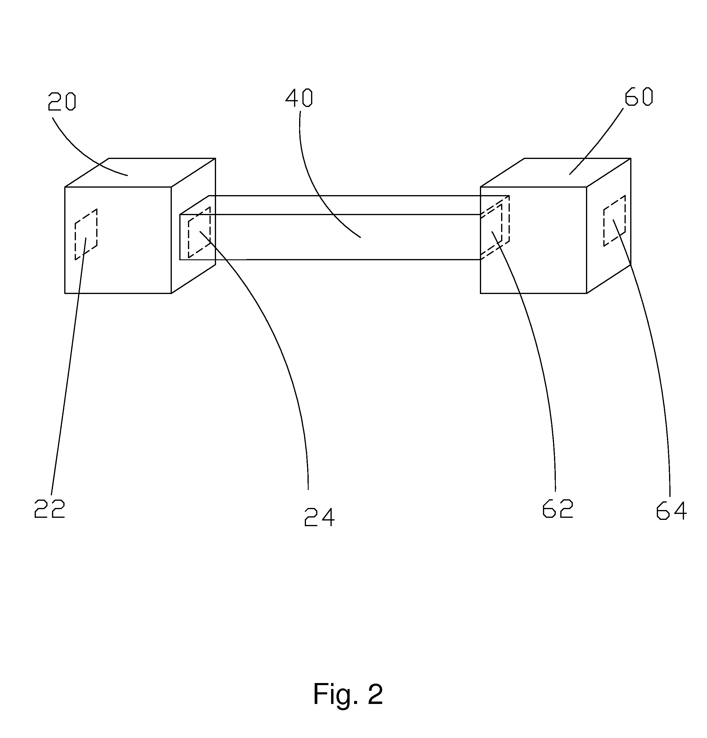
[0036]Step 1: Provide a substrate 10 waiting for a pretreatment, an UV chamber 20 and a loading chamber 60.
[0037]The substrate 10 is an OLED substrate, and the pretreatment is the coating pretreatment.
[0038]Step 2: Provide a transfer chamber 40 between the UV chamber 20 and the loading chamber 60 to connect the UV chamber 20 and the loading chamber 60, provide a first sealing door 24 at a place where the UV chamber 20 and the transfer chamber 40 are connected with each other, and provide a second sealing door 62 at a place where the transfer chamber 40 and the loading chamber 60 are connected with each other, wherein the transfer chamber 40 is a hermetically sealed chamber after ...
PUM
 Abstract
Description
Claims
Application Information