Semiconductor module and method for manufacturing the same

a technology of semiconductor and module, applied in the direction of semiconductor/solid-state device details, semiconductor devices, electrical apparatus, etc., can solve the problems of reducing bonding strength, increasing equipment cost, and complicated pressing jigs

Active Publication Date: 2016-09-01
FUJI ELECTRIC CO LTD
View PDF7 Cites 12 Cited by
  • Summary
  • Abstract
  • Description
  • Claims
  • Application Information

AI Technical Summary

Problems solved by technology

In a state where a lead terminal is floating from the case, in attempting to ultrasonically bond a bonding wire to the lead terminal, the ultrasonic vibration energy will be absorbed by the lead terminal, which causes a bonding defect.
The adhesive flowing out to the outside of the case will deteriorate the appearance of the case, and furthermore the adhesive flowing into the case will contaminate the bonding portion formed by ultrasonic bonding and reduce the bonding strength.
The conventional semiconductor module has a problem that the equipment cost increases because when a bonding wire is ultrasonically bonded to a lead frame, a pin-like pressing jig is needed for pressing the face opposite to an ultrasonic bonding face and in addition the pressing jig is complicated.
Moreover, there is also a problem that the manufacturing throughput decreases because the pressing jig needs to be attached and detached in ultrasonic bonding and thus the attachment and detachment take a time.

Method used


Image

  • Semiconductor module and method for manufacturing the same
  • Semiconductor module and method for manufacturing the same
  • Semiconductor module and method for manufacturing the same

Examples


Embodiment Construction

[0026]Hereinafter, embodiments of a semiconductor module according one aspect will be described in detail with reference to the accompanying drawings. Note that, in the drawing used for description of the following embodiments, the same constituent element is given the same reference numeral to omit the duplicated description.

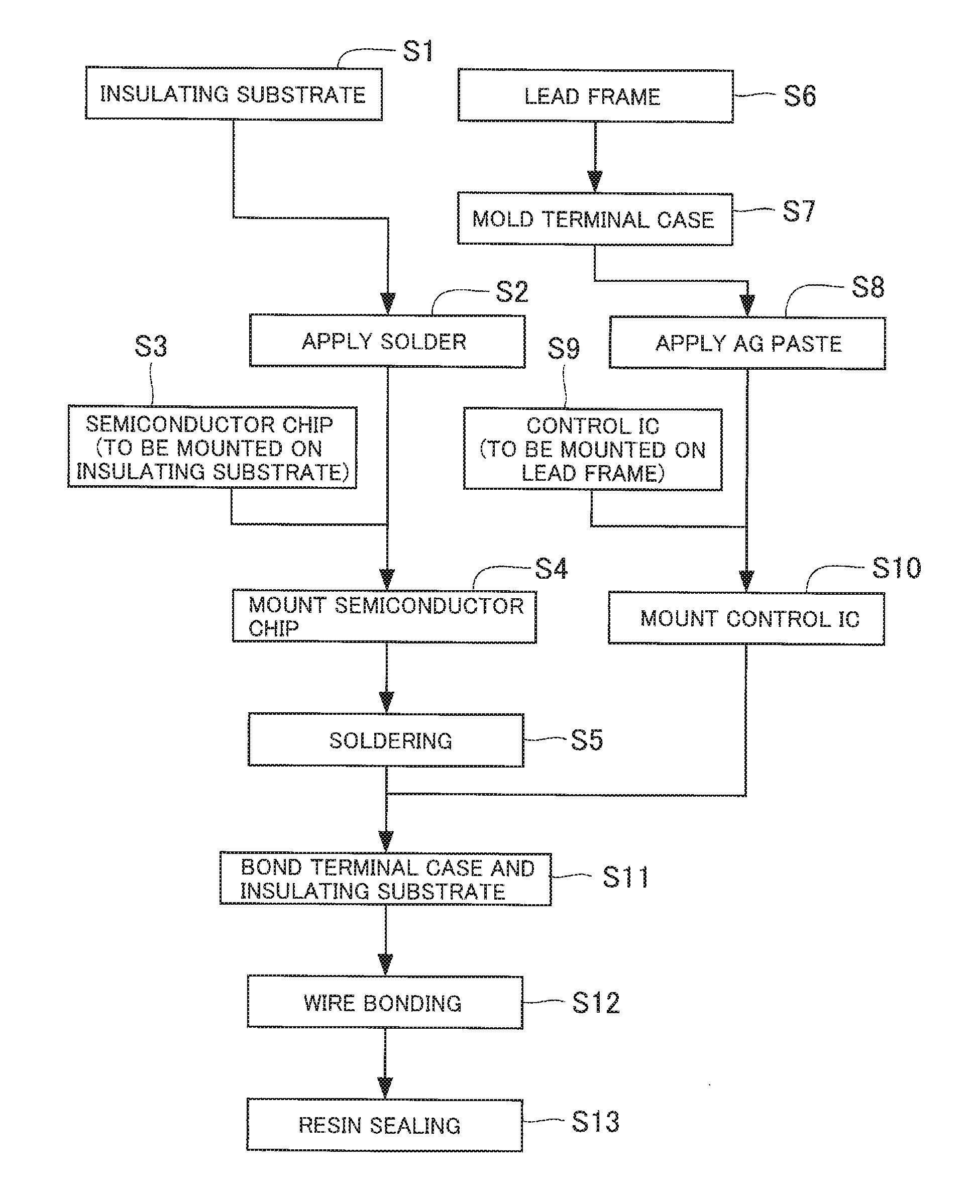
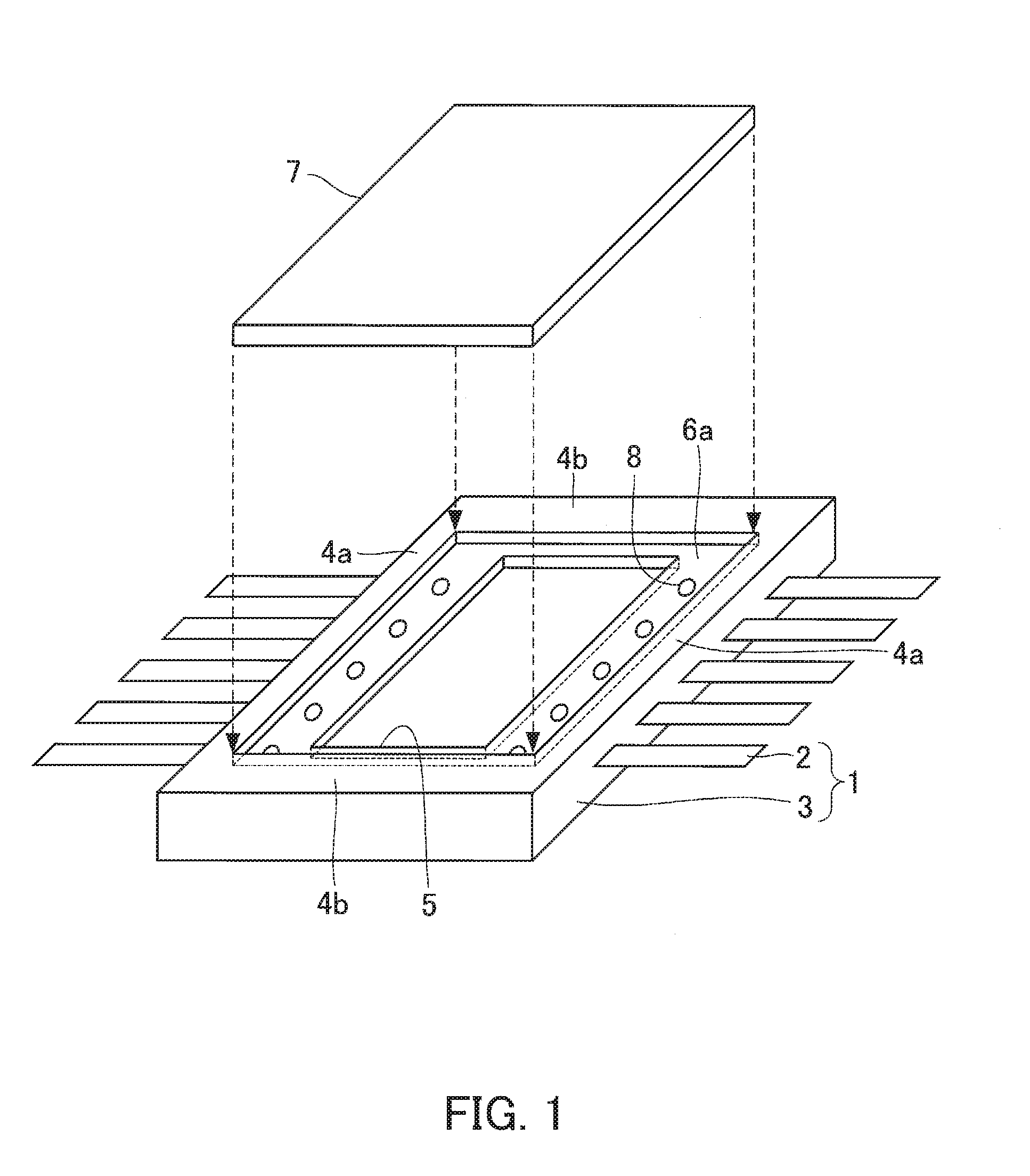
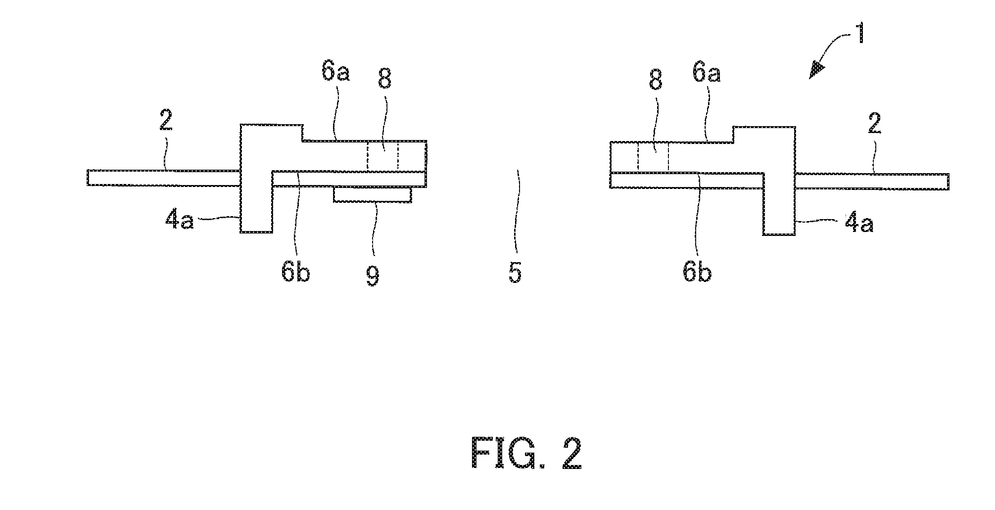
[0027]FIG. 1 is an exploded perspective view of a semiconductor module according to an embodiment discussed herein when seen from the bottom-face side of the semiconductor module, FIG. 2 is a cross sectional view illustrating the semiconductor module in an upside down state before mounting of an insulating substrate, FIG. 3 is a cross sectional view illustrating the semiconductor module at mounting of the insulating substrate, FIG. 4 is a cross sectional view illustrating the semiconductor module when wiring with a bonding wire is performed, and FIG. 5 is a cross sectional view illustrating the semiconductor module after resin sealing.

[0028]The semiconductor mo...


PUM


Abstract

A terminal case formed by integrally molding a lead frame and a case that has internally an inner face on which the lead frame is mounted and has externally a step portion fixed to a circuit block having an insulating substrate and semiconductor chips formed on the insulating substrate. An opening portion is formed between the step portion and the inner face so as to extend through them, and the opening portion is filled with an adhesive to bond the insulating substrate to the step portion. Since a connecting area to which a bonding wire of the lead frame is ultrasonically bonded is fixed, it is possible to reduce the bonding failures of the lead frames.

Description

CROSS-REFERENCE TO RELATED APPLICATION[0001]This application is a continuation application of International Application PCT / JP2015 / 055066 filed on Feb. 23, 2015 which designated the U.S., which claims priority to Japanese Patent Application No. 2014-093422, filed on Apr. 30, 2014, the entire contents of which are incorporated herein by reference.BACKGROUND OF THE INVENTION[0002]1. Field of the Invention[0003]Embodiments discussed herein relate to a semiconductor module and a method for manufacturing the same. In particular, they relate to a semiconductor module used in applications including an inverter device, such as a motor drive device, and a power conversion device, such as a switching power supply device, and to the method for manufacturing the same.[0004]2. Background of the Related Art[0005]In a semiconductor module for power conversion, a plurality of semiconductor chips for power, such as power transistors or diodes for power conversion, is integrated into one package. In ...

Claims


Application Information

Patent Timeline
Patent Type & Authority Applications(United States)
IPC IPC(8): H01L23/495H01L21/52H01L21/48H01L21/56H01L23/04H01L23/31
CPCH01L23/49541H01L23/04H01L23/4952H01L23/49506H01L21/4871H01L21/4825H01L21/565H01L21/52H01L23/3142H01L25/18H01L2224/48137H01L2224/48472H01L2224/4903H01L2224/49171H01L2924/19107H01L23/057H01L25/072H01L2224/32225H01L2224/32245H01L2224/48247H01L2224/73265H01L2224/85205H01L2224/92247H01L2924/13055H01L2924/13091H01L2924/14H01L2924/181H01L2224/48139H01L24/85H01L24/29H01L24/48H01L24/49H01L24/83H01L24/92H01L2224/29339H01L2224/45124H01L2224/83192H01L2224/8321H01L2924/00014H01L2224/29101H01L2224/48096H01L2924/00012H01L2924/00H01L2224/05599H01L2924/014
Inventor SATO, TADAHIKO
Owner FUJI ELECTRIC CO LTD
Why Eureka
Try Eureka