Thin film transistor substrate and method of manufacturing the same

Active Publication Date: 2016-09-08
SAMSUNG DISPLAY CO LTD
View PDF2 Cites 3 Cited by
  • Summary
  • Abstract
  • Description
  • Claims
  • Application Information

AI Technical Summary

Benefits of technology

[0010]Exemplary embodiments of the present disclosure provide a display substrate capable of decre

Problems solved by technology

When the organic layer is exposed, a surface of the organic

Method used


Image

  • Thin film transistor substrate and method of manufacturing the same
  • Thin film transistor substrate and method of manufacturing the same
  • Thin film transistor substrate and method of manufacturing the same

Examples


Example

[0043]Hereinafter, the present disclosure will be explained in detail with reference to the accompanying drawings.

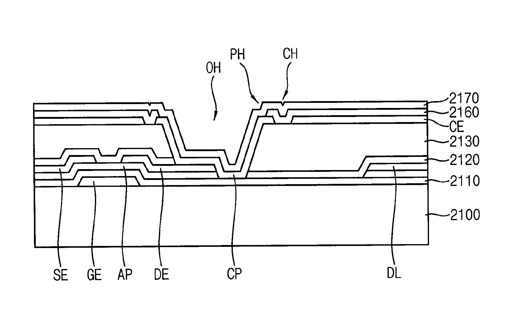
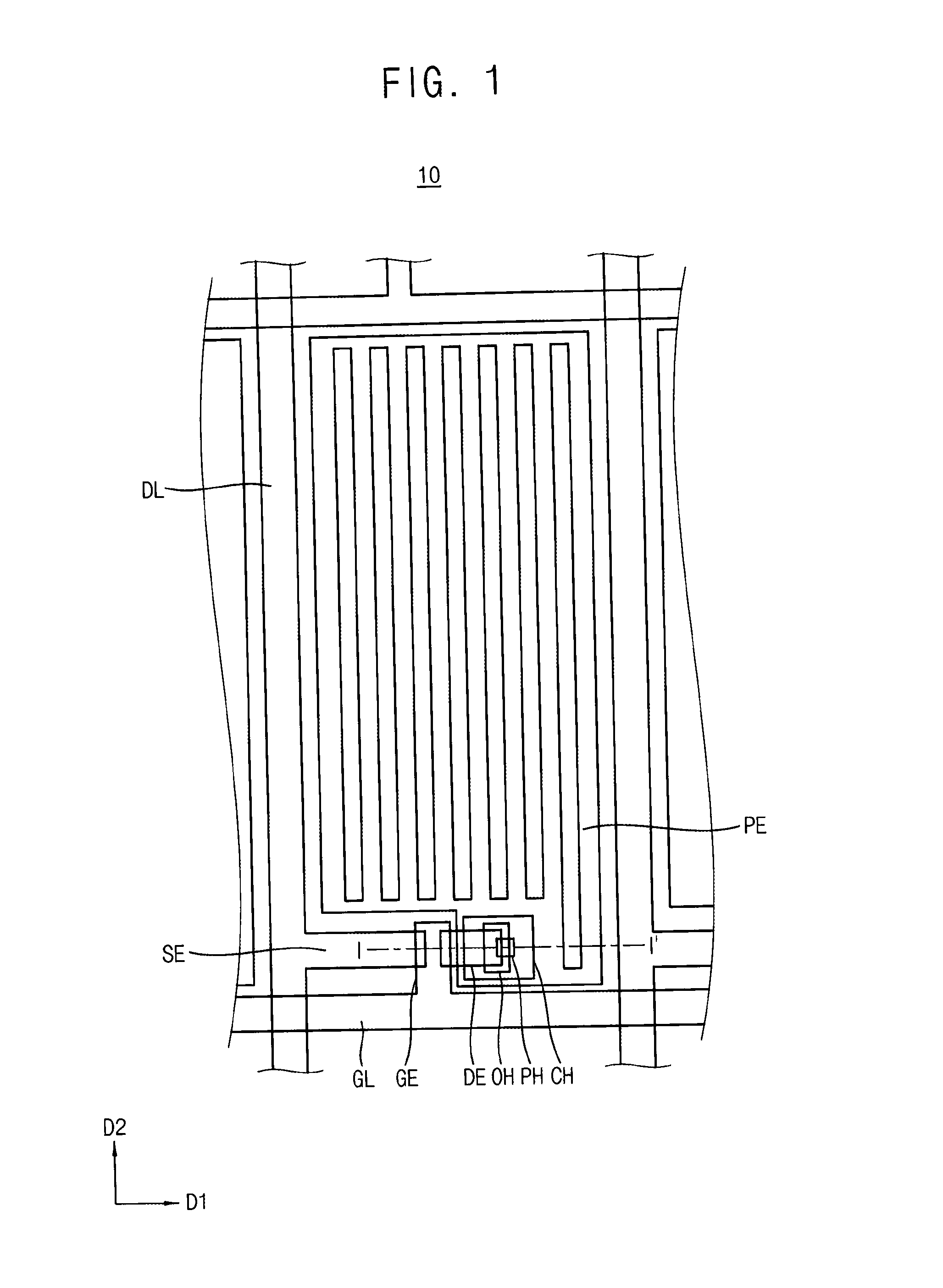
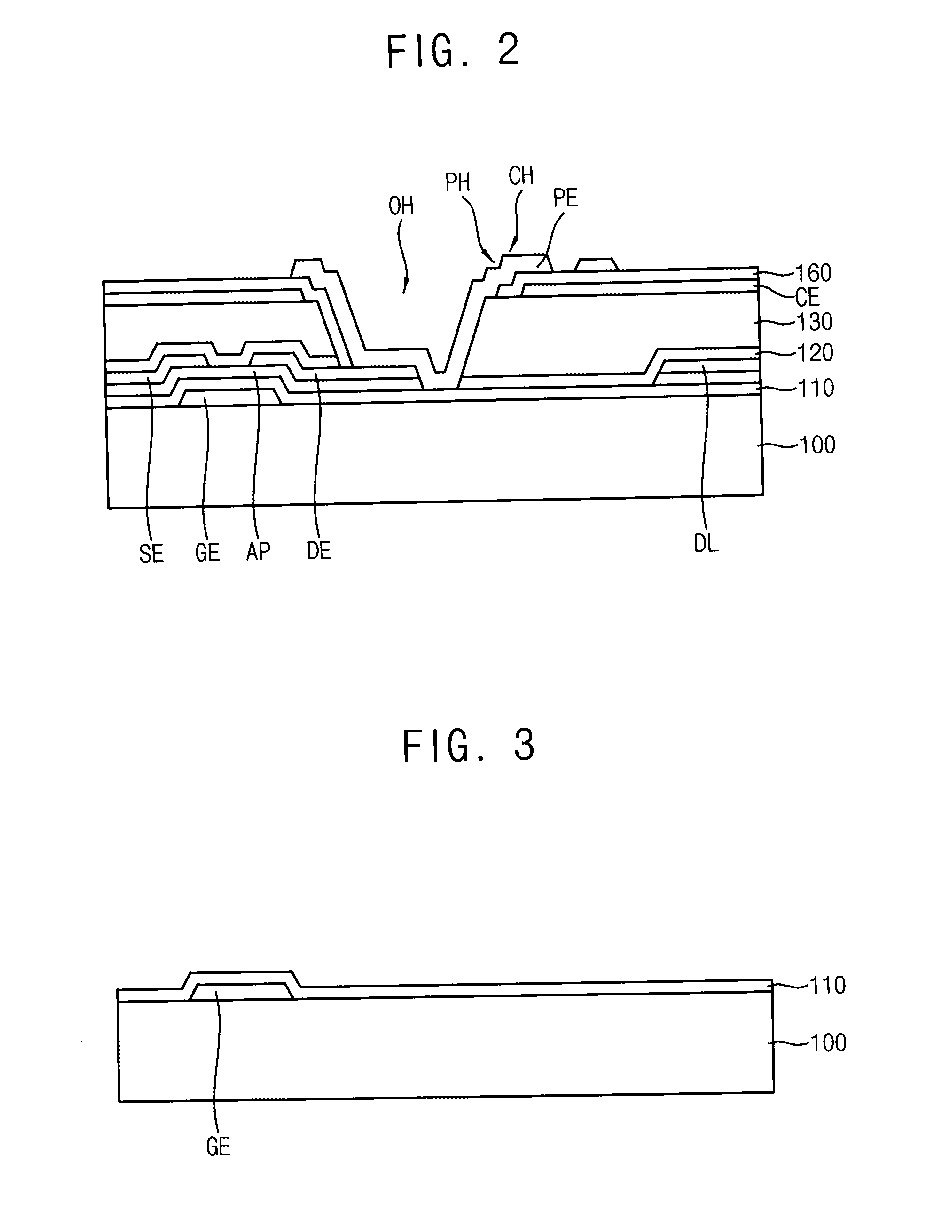
[0044]FIG. 1 is a plan view illustrating a thin film transistor substrate according to an exemplary embodiment of the present disclosure. FIG. 2 is a cross-sectional view taken along the line I-I′ of FIG. 1. Referring to FIGS. 1 and 2, a thin film transistor substrate 10 according to an exemplary embodiment includes a base substrate 100, a gate metal pattern including a gate line GL and gate electrode GE, a data metal pattern including a data line DL, a gate insulation 110, an active pattern AP, a first passivation layer 120, an organic layer 130, a common electrode CE, a second passivation layer 160, and pixel electrode PE. The gate line GL extends in a first direction D1. In one embodiment, the gate line GL has a single layer structure including copper (Cu), silver (Ag), chrome (Cr), molybdenum (Mo), aluminum (Al), titanium (Ti), manganese (Mn), and a mixture thereof. ...


PUM


Abstract

A thin film transistor substrate includes a switching element comprising a gate electrode electrically connected to a gate line extending in a first direction, an active pattern overlapping with the gate electrode, a source electrode disposed on the active pattern and electrically connected to a data line extending in a second direction crossing the first direction, and a drain electrode spaced apart from the source electrode. The thin film transistor substrate further includes an organic layer disposed on the switching element, a first electrode disposed on the organic layer, and a second electrode overlapping with the first electrode, and electrically connected to the drain electrode. A thickness of the second electrode is thicker than a thickness of the first electrode.

Description

CROSS-REFERENCE TO RELATED APPLICATIONS[0001]This application claims priority under 35 U.S.C. §119 to Korean Patent Application No. 10-2015-0030485, filed on Mar. 4, 2015 in the Korean Intellectual Property Office KIPO, the disclosure of which is herein incorporated by reference in its entirety.BACKGROUND[0002]1. Field[0003]Exemplary embodiments of the present disclosure relate to thin film transistor substrate and a method of manufacturing the thin film transistor substrate.[0004]2. Description of the Related Art[0005]Generally, a liquid crystal display (LCD) apparatus includes a display substrate, an upper substrate, and a liquid crystal layer interposed between the display substrate and the upper substrate. A plurality of signal lines and a plurality of thin film transistor are formed on the display substrate.[0006]To display an image on the LCD apparatus, a liquid crystal display panel generally uses a twisted nematic (TN) mode. To ensure a wide viewing angle, the liquid crystal...

Claims


Application Information

Patent Timeline
IPC IPC(8): H01L27/12H01L29/66H01L21/311H01L29/786
CPCH01L27/1248H01L27/124H01L21/31111H01L29/66765H01L27/127H01L29/78669G02F1/1362H01L21/84H01L27/12H01L27/1214H01L27/1259H01L21/31116H01L29/78618H01L2924/13069H01L29/41733G02F1/136227
Inventor KIM, BYOUNG-YONGJEON, WOONG-KIKIM, HYUN-JINSONG, JEAN-HO
Owner SAMSUNG DISPLAY CO LTD
Why Eureka
Try Eureka