Pixel unit, method of manufacturing the same and display device

Active Publication Date: 2016-09-08
BOE TECH GRP CO LTD
View PDF1 Cites 3 Cited by
  • Summary
  • Abstract
  • Description
  • Claims
  • Application Information

AI Technical Summary

Benefits of technology

[0024]In the present invention, the pixel definition layer is formed or provided as a plurality of pixel definition units that are spaced from each other. Compared to the prior art, the thickness of the pixel definition layer surrounding the organic light-emitting layer is thinned, such that the light path of the light emitted from the organic light-emitting layer within the pixel definition units is shortened. The present invention increases the area of the pixel anode by reducing the spacing between any two adjacent pixel anodes. At the same time, since the thickness of the pixel definition layer is thinned, when the light emitted from

Problems solved by technology

At present, light extraction efficiency of the OLED device is mainly restricted by the following two factors:1. Total reflection of the light at an electrode-air interface and a glass-air interface will restrict light extraction, because difference in refractive index between different medium materials is great; such difference in refractive index causes only light rays emitted from a light-emitting point so

Method used


Image

  • Pixel unit, method of manufacturing the same and display device
  • Pixel unit, method of manufacturing the same and display device
  • Pixel unit, method of manufacturing the same and display device

Examples


Embodiment Construction

[0030]Purposes, technical schemes and advantages of the present invention will become more apparent by explaining embodiments of the present invention, in combination with the accompanying drawings, in detail.

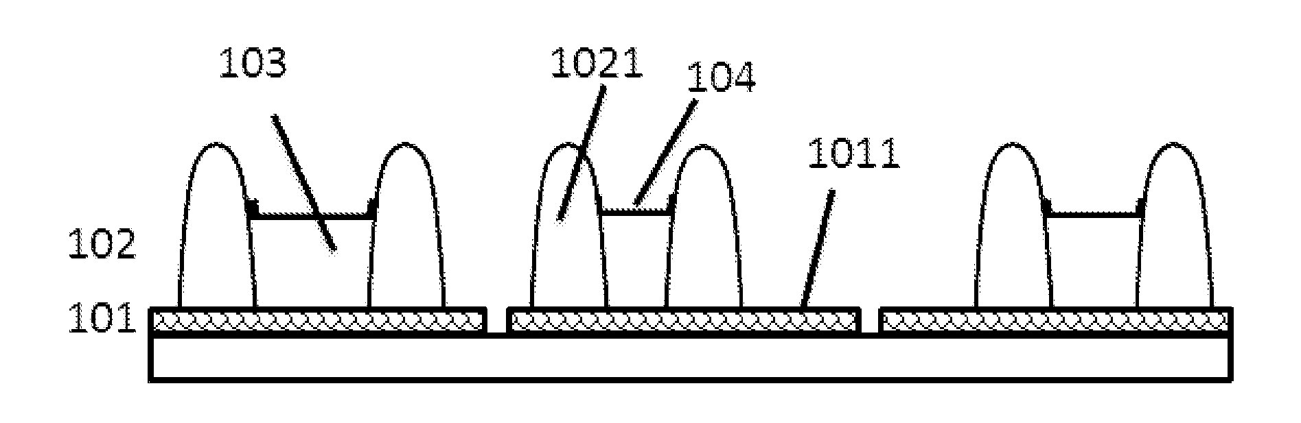
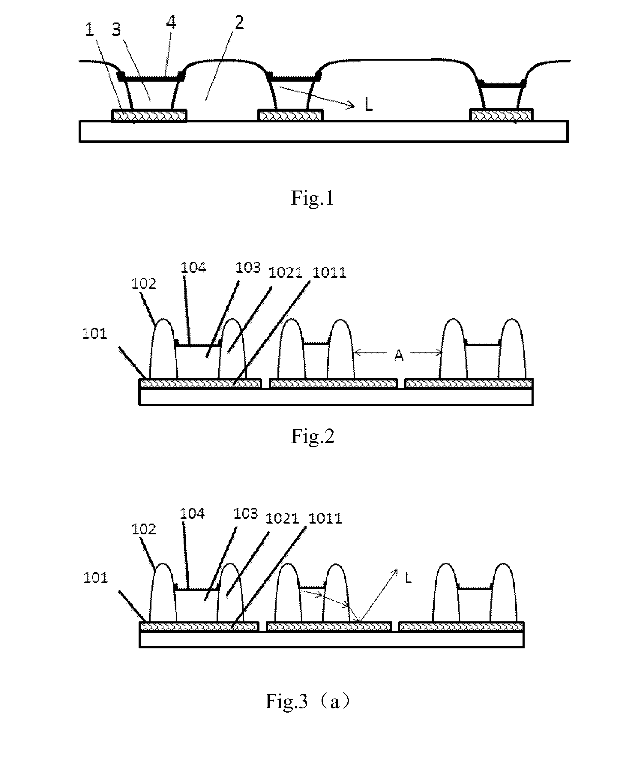
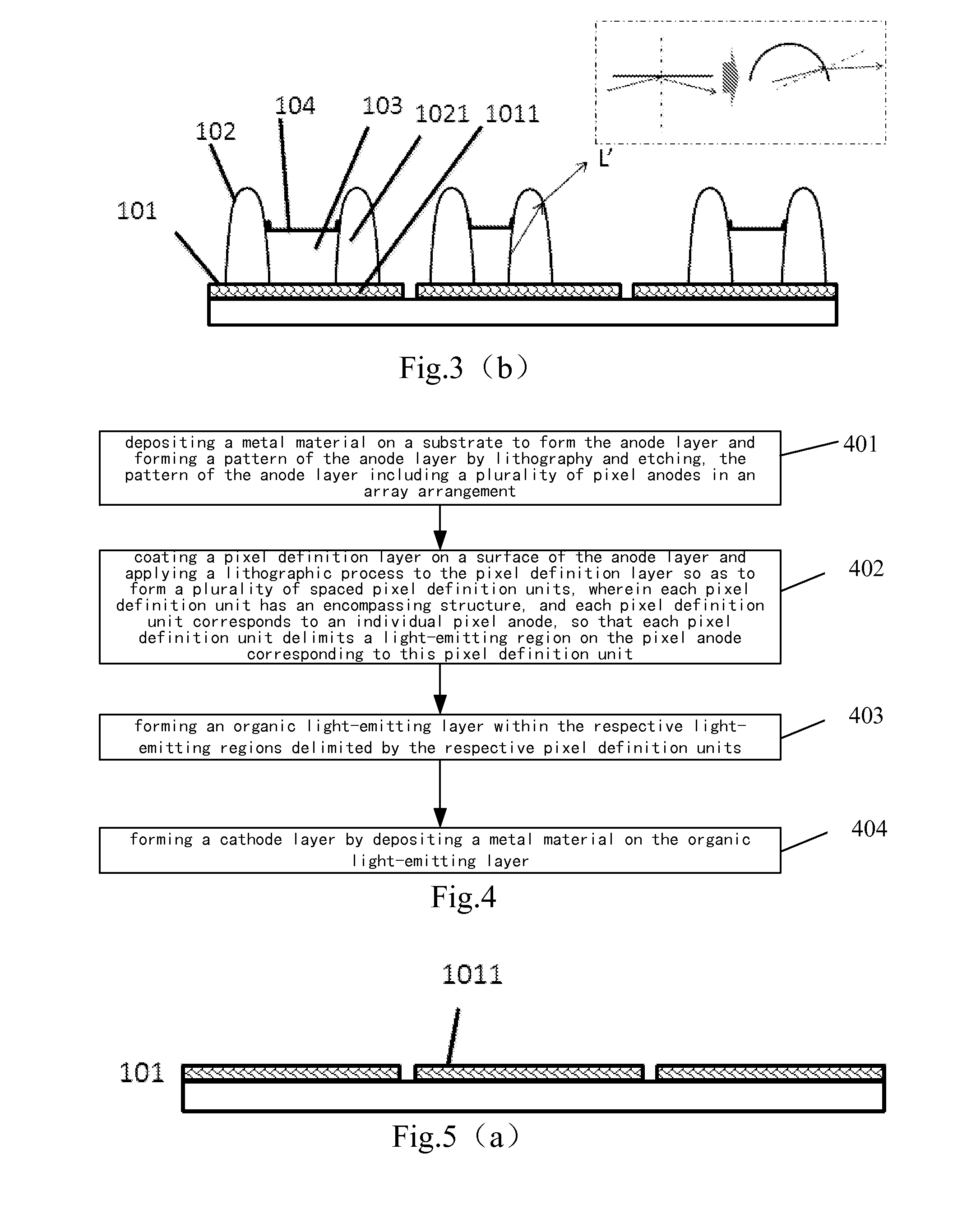
[0031]In order to solve the problems in the prior art that the structure of the pixel definition layer adversely influences an extraction efficiency of a side exiting light, the light reflected by the anode is transmitted within the pixel definition layer through a longer light path and much energy of the reflected light is absorbed by the material, and the light is totally reflected when exiting the pixel definition layer and loss of the exiting light occurs, the present invention provides a pixel unit and a method of manufacturing the same, and a display device, which can shorten a light path of the light within the pixel definition layer, reduce light absorbing, prevent total reflection, improve light extraction efficiency of the OLED device, and hence improve external quant...


PUM


Abstract

The present invention discloses a pixel unit, a method of manufacturing the same and a display device. The pixel unit comprises an anode layer, a pixel definition layer, an organic light-emitting layer and a cathode layer, wherein the anode layer includes a plurality of pixel anodes in an array arrangement, and the pixel definition layer is disposed on the anode layer and includes a plurality of spaced pixel definition units, wherein the pixel definition units correspond to the pixel anodes one by one, and each pixel definition unit delimits a light-emitting region on the corresponding pixel anode, and the organic light-emitting layer is provided within the light-emitting regions, and the cathode layer is provided on the organic light-emitting layer. The present invention remarkably increases light extraction efficiency by improving the structure of the pixel unit.

Description

BACKGROUND OF THE INVENTION[0001]1. Field of the Invention[0002]The present disclosure relates to the technical field of display, and in particular, to a pixel unit, a method of manufacturing the same and a display device.[0003]2. Description of the Related Art[0004]A basic structure of an Organic Light-Emitting Diode (OLED) device is of a sandwich-like structure formed by connecting a thin and transparent layer of Indium Tin Oxide (ITO) to an anode of a power supply and providing a metal cathode, wherein the ITO layer has semiconductor characteristics. The whole structure comprises a hole transmission layer (HTL), a light-emitting layer (EL) and an electron transmission layer (ETL). When the power supply supplies a suitable voltage, holes of the anode and charges of the cathode will combine with each other in the light-emitting layer to generate light. Light with three primary colors, i.e., red color, green color and blue color (RGB), can be generated according to different recipes...

Claims


Application Information

Patent Timeline
IPC IPC(8): H01L27/32H01L51/52H01L51/00H01L51/56
CPCH01L27/3246H01L51/0023H01L51/5206H01L51/56H10K59/10H10K59/122H10K71/621H10K50/813H10K50/818H10K50/822H10K71/00H10K50/81
Inventor SHI, LEIHUANGFU, LUJIANGXU, XIAOWEI
Owner BOE TECH GRP CO LTD
Why Eureka
Try Eureka