Light emitting device

a technology of light emitting device and light source, which is applied in the direction of organic semiconductor device, semiconductor device, electrical apparatus, etc., to achieve the effect of improving light emission quality

Inactive Publication Date: 2016-09-15
OLEDWORKS GMBH
View PDF4 Cites 3 Cited by
  • Summary
  • Abstract
  • Description
  • Claims
  • Application Information

AI Technical Summary

Benefits of technology

[0003]It is an object of the present invention to provide a light emitting device having an improved light emission quality. It is a further object of the present invention to provide a layer structure that can be used to produce the light emitting device, and to provide a production method for producing the layer structure.

Problems solved by technology

However, if such a scattering function is added to the device, then absorption of light by any of the further layers of the device plays a much bigger role, for example due to scattering processes and increased lengths of light paths, which is especially true for the transparent anode layer.

Method used


Image

  • Light emitting device
  • Light emitting device
  • Light emitting device

Examples


Embodiment Construction

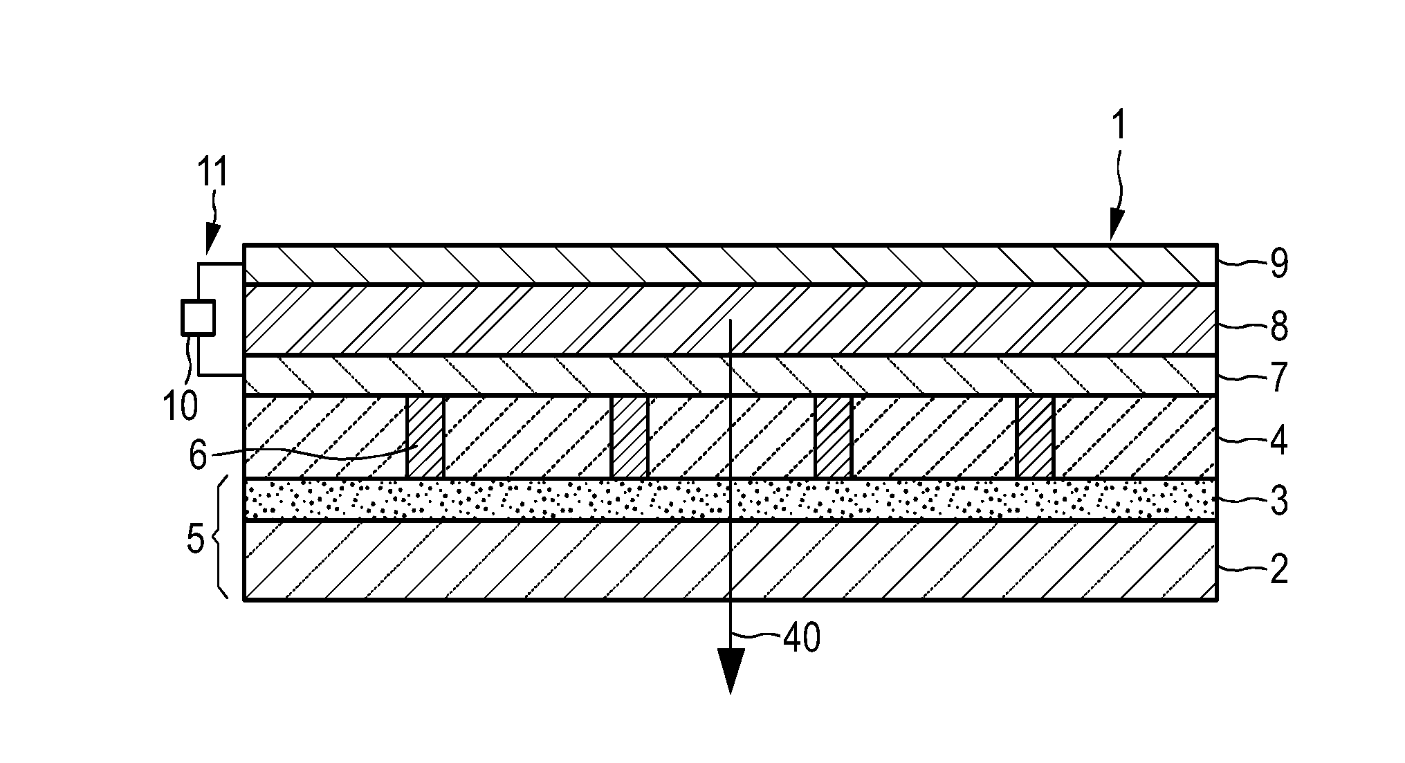
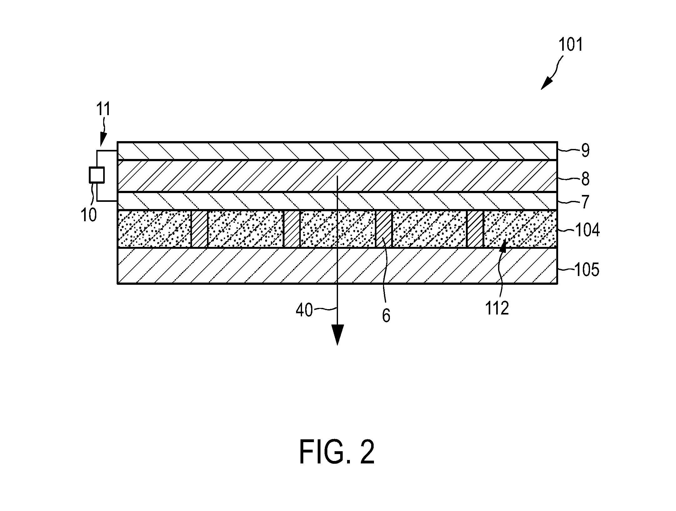
[0021]FIG. 1 shows schematically and exemplarily an embodiment of a light emitting device. The light emitting device 1 is an OLED comprising an organic light emitting layer 8 between a first electrode layer being a transparent anode layer 7 and a second electrode layer being a reflective cathode layer 9. A voltage source 10 is connected to the anode layer 7 and the cathode layer 9 via electrical connections 11 like wires, wherein the organic light emitting layer 8 is adapted to emit light 40, if the voltage is applied to the anode layer 7 and the cathode layer 9.

[0022]The organic light emitting layer 8 comprises a stack of sublayers including one or several organic light emitting sublayers and optionally further sublayers like one or several hole injection sublayers, one or several hole transport sublayers, one or several electron transport sublayers, one or several charge generation sublayers, et cetera. The OLED 1 further comprises a substrate 5, which might be a glass substrate o...


PUM


Abstract

The invention relates to a light emitting device (1) comprising a substrate (5), a transparent anode layer (7), a cathode layer (9), a light emitting layer (8) between the anode and cathode layers, and an intermediate layer (4) between the substrate and the anode layer. An electrically conducting element is embedded in the intermediate layer such that it is in contact with the anode layer. Also, scattering particles for scattering the light are embedded in the intermediate layer, increasing the light outcoupling efficiency of the device. Since the electrically conducting element is embedded in the intermediate layer and not, for instance, on top of the anode layer, i.e. not in between the anode and cathode layers, the sheet resistance of the anode layer can be reduced, without requiring a passivation layer which may adversely affect the light emitting material. Furthermore, the embedded electrically conducting element allows the thickness of the transparent anode layer to be reduced to a thickness of about 50 nm or less, thereby minimizing the influence of light absorption by the transparent anode layer on the light outcoupling efficiency. This allows for an improved light emission quality.

Description

FIELD OF THE INVENTION[0001]The invention relates to a light emitting device, a layer structure for being used to produce the light emitting device and a production method for producing the layer structure.BACKGROUND OF THE INVENTION[0002]An organic light emitting device (OLED) comprises a substrate like a glass substrate with an anode layer, a cathode layer and an organic light emitting layer in between the anode layer and the cathode layer, wherein the organic light emitting layer is adapted to emit light, if voltage is applied to the anode layer and the cathode layer. Moreover, on top of the anode layer, i.e. within the organic light emitting layer, a metallic grid may be provided, in order to reduce the sheet resistance of the anode layer, wherein on top of the metal grid a passivation layer like a photoresist layer can be provided, in order to suppress electrical shorts in the OLED. However, the organic light emitting layer may be adversely affected by humidity and by reactions...

Claims


Application Information

Patent Timeline
Patent Type & Authority Applications(United States)
IPC IPC(8): H01L51/52
CPCH01L51/5212H01L51/5268H01L2251/558H01L51/5231H01L51/5275H10K50/814H10K50/854H10K50/858H10K2102/351H10K71/00H10K50/826
Inventor SCHWAB, HOLGERRUSKE, MANFRED
Owner OLEDWORKS GMBH
Why Eureka
Try Eureka