

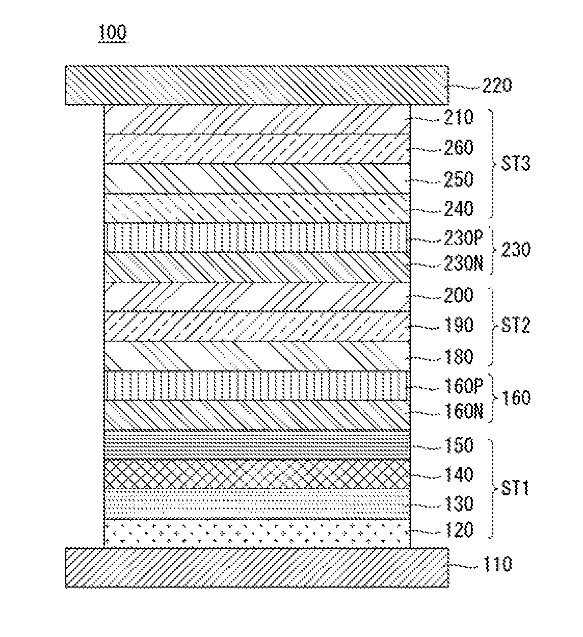
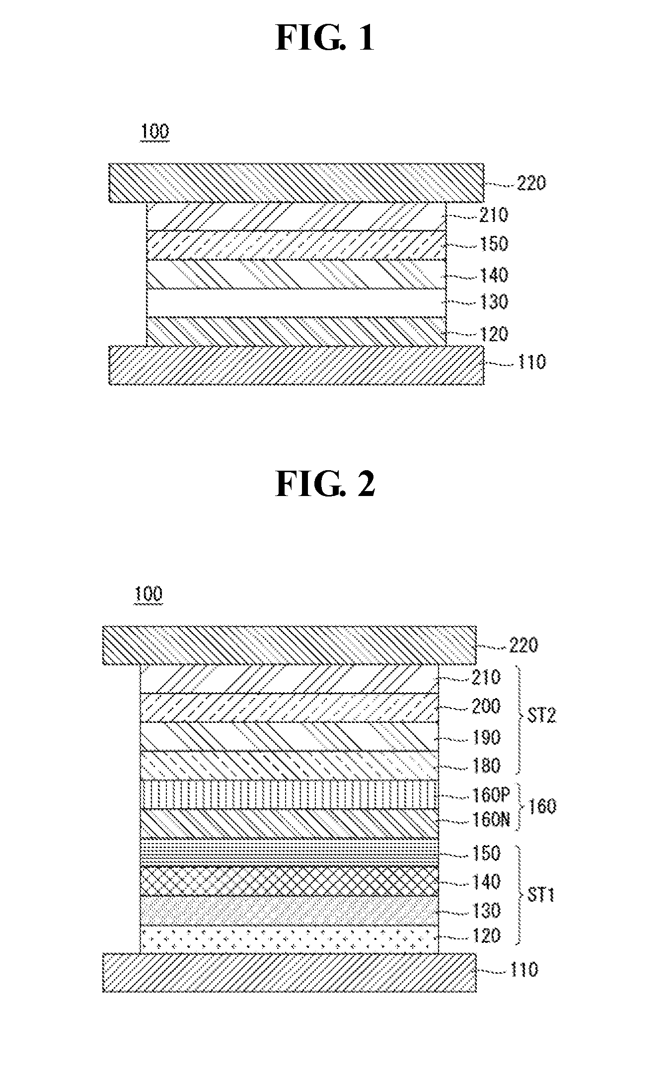
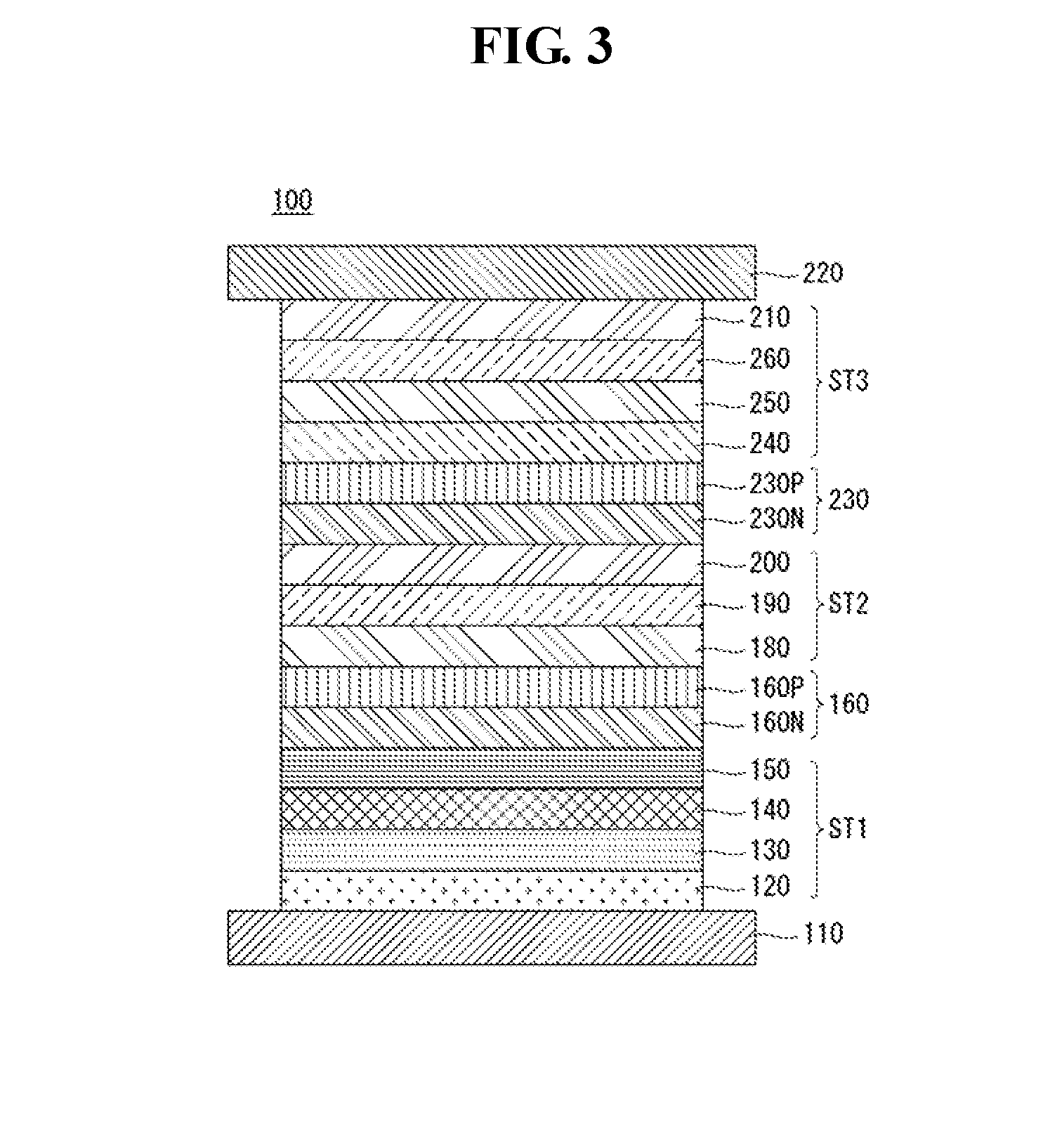
Organic light emitting display device
a light-emitting display and organic technology, applied in the direction of luminescent compositions, semiconductor devices, luminescent compositions, etc., can solve the problems of increasing operating voltage, reducing efficiency of multi-layer emitting devices compared to single-layer emitting structures, etc., to improve light emission efficiency, reduce operating voltage, and improve electron injection
- Summary
- Abstract
- Description
- Claims
- Application Information
AI Technical Summary
Benefits of technology
Problems solved by technology
Method used
Image

Examples
embodiment 1
[0113]It has the same elements as the above-described Comparative Example 1, and the electron transport layer was formed of the following compound Pn2-A07.
embodiment 2
[0115]It has the same elements as the above-described Comparative Example 2, and the second electron transport layer was formed from the above Compound Pn2-A07.
[0116]The materials for the electron transport layer in the above Comparative Examples and Embodiments do not limit the scope of the present disclosure.
[0117]The operating voltage and efficiency of the devices manufactured according to the above-described Comparative Examples and Embodiments were measured and shown in the following Table 1. (The measurements taken in Embodiments were expressed as a percentage relative to those taken in Comparative Examples corresponding to 100%, and the devices manufactured according to Comparative Examples and Embodiments were driven at an operating current of 10 mA / cm2).
[0118]The current density vs voltage of the organic light emitting display devices manufactured according to Comparative Example 1 and Embodiment 1 was measured and shown in FIG. 5, and the efficiency vs luminance was measur...
PUM
 Abstract
Description
Claims
Application Information