

Electron injection composition for light emitting element, light emitting element, and light emitting device
- Summary
- Abstract
- Description
- Claims
- Application Information
AI Technical Summary
Benefits of technology
Problems solved by technology
Method used
Image

Examples
embodiment 1
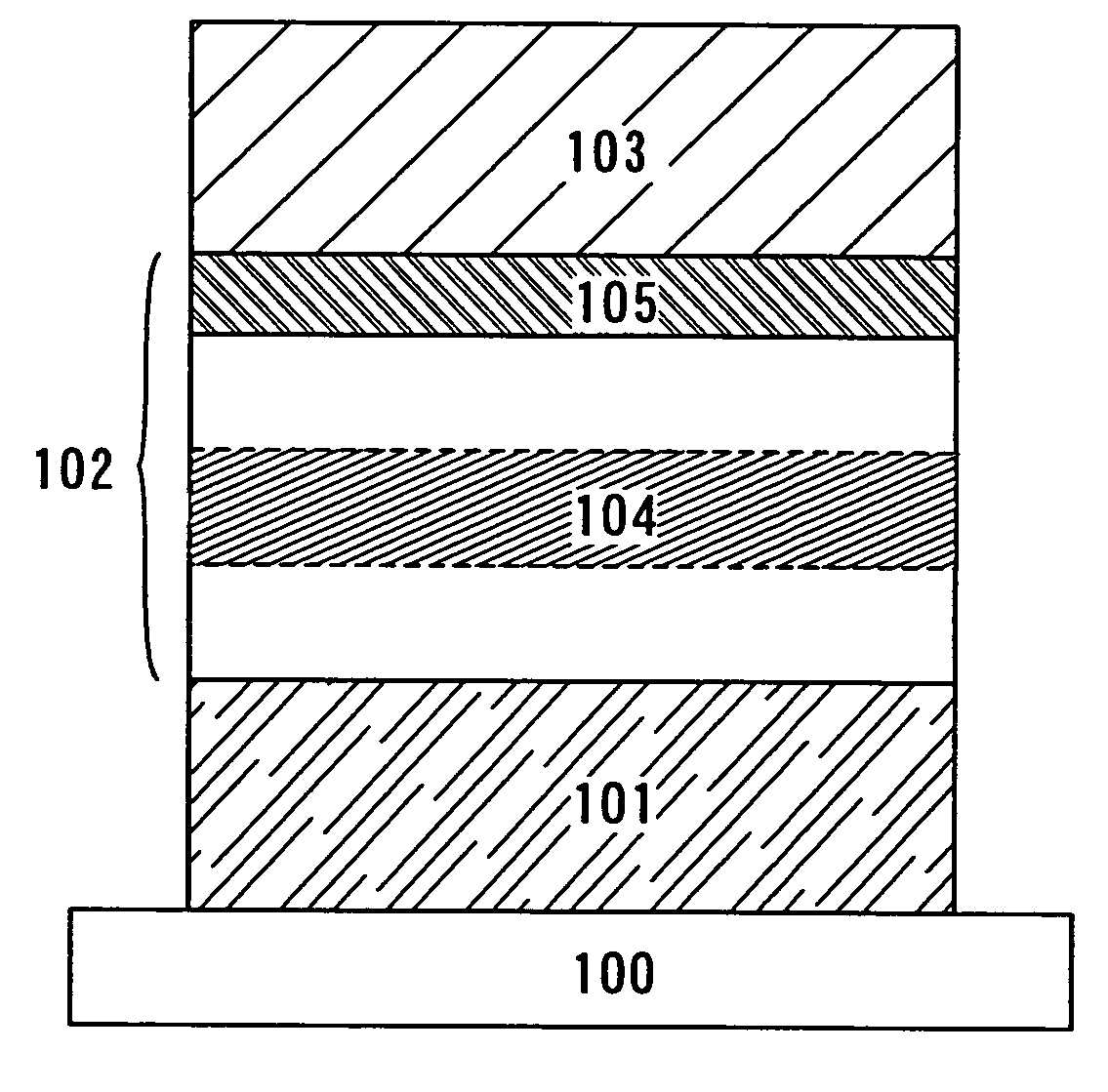
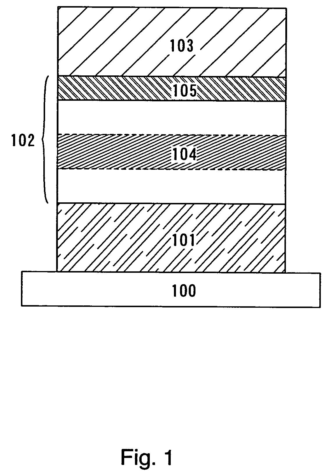
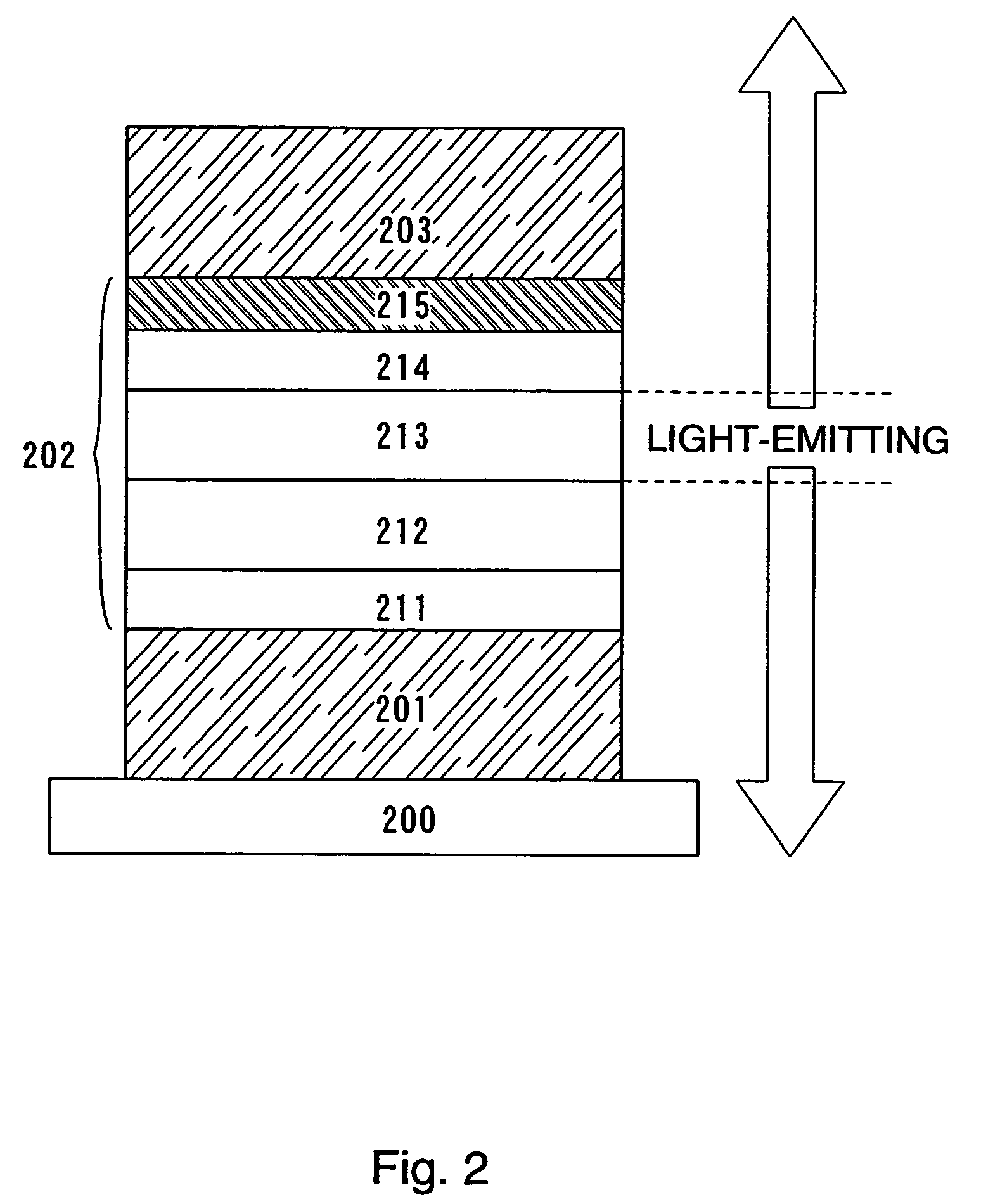
[0056]In the present embodiment, a light-emitting element according to the present invention in the case of a structure in which light generated in a layer including a luminescent material is emitted from both side of first and second electrodes of a light-emitting element (hereinafter, referred to as a both-emission structure), which has an electron injection layer provided in a portion of the layer including the luminescent material, will be described with reference to FIG. 2.
[0057]First, a first electrode 201 of a light-emitting element is formed on a substrate 200. In the present embodiment, the first electrode 201 functions as an anode. ITO that is a transparent conductive film is used as a material to form the first electrode 201 with a film thickness of 110 nm by sputtering.
[0058]Next, a layer 202 including a luminescent material is formed on the first electrode (anode) 201. The layer 202 including the luminescent material in the present embodiment has a laminated structure c...
embodiment 2
[0073]In the present embodiment, a specific structure in which light is emitted from a second electrode to be formed a layer including a luminescent material (hereinafter, referred to as a top-emission structure) in the case of a structure where light generated in a layer including a luminescent material is emitted from one side of a light-emitting element will be described with reference to FIG. 3.
[0074]Only different portion from the structure in Embodiment 1 will be described here, and descriptions of component parts except a first electrode, which are the same as those of Embodiment 1, will be omitted.
[0075]A first electrode 301 in the present embodiment functions as an anode, from which no light generated in a layer 302 including a luminescent material is emitted. In other words, a nitride or carbide of an element belonging to one of Group 4, Group 5, and Group 6 of the periodic table of the elements, which has a large work function and shields light, such as titanium nitride, ...
embodiment 3
[0081]In the present invention, a structure in which light is emitted from a side of an electron injection layer 515 included in a layer 502 including a luminescent material as shown in FIG. 4 (hereinafter, referred to as a top-emission structure) can also be employed in the case of a structure where light generated in a layer including a luminescent material is emitted from one side of a light-emitting element as described in Embodiment 2.
[0082]In the same way as Embodiment 2, as a first electrode 501, a reflective conductive film 504 is formed on a substrate 500 and then, a transparent conductive film 505 is formed thereon. After forming the first electrode 501, a hole injection layer 511, a hole transport layer 512, a light-emitting layer 513, an electron transport layer 514, the electron injection layer 515, and a second electrode 503 are sequentially laminated in the same way as Embodiments 1 and 2.
[0083]In the case of the present embodiment, since the second electrode (cathode...
PUM
| Property | Measurement | Unit |
|---|---|---|
| Fraction | aaaaa | aaaaa |
| Ratio | aaaaa | aaaaa |
| Molar ratio | aaaaa | aaaaa |
Abstract
Description
Claims
Application Information