Electron injection composition for light emitting element, light emitting element, and light emitting device
a technology of light emitting elements and compositions, applied in thermoelectric devices, discharge tubes luminescnet screens, natural mineral layered products, etc., can solve the problems of difficult to keep amorphous, difficult to crystallize with time, and few suitable materials for forming transparent conductive films, etc., to achieve superior injection effect, superior characteristics, and easy crystallization with time
- Summary
- Abstract
- Description
- Claims
- Application Information
AI Technical Summary
Benefits of technology
Problems solved by technology
Method used
Image
Examples
embodiment 1
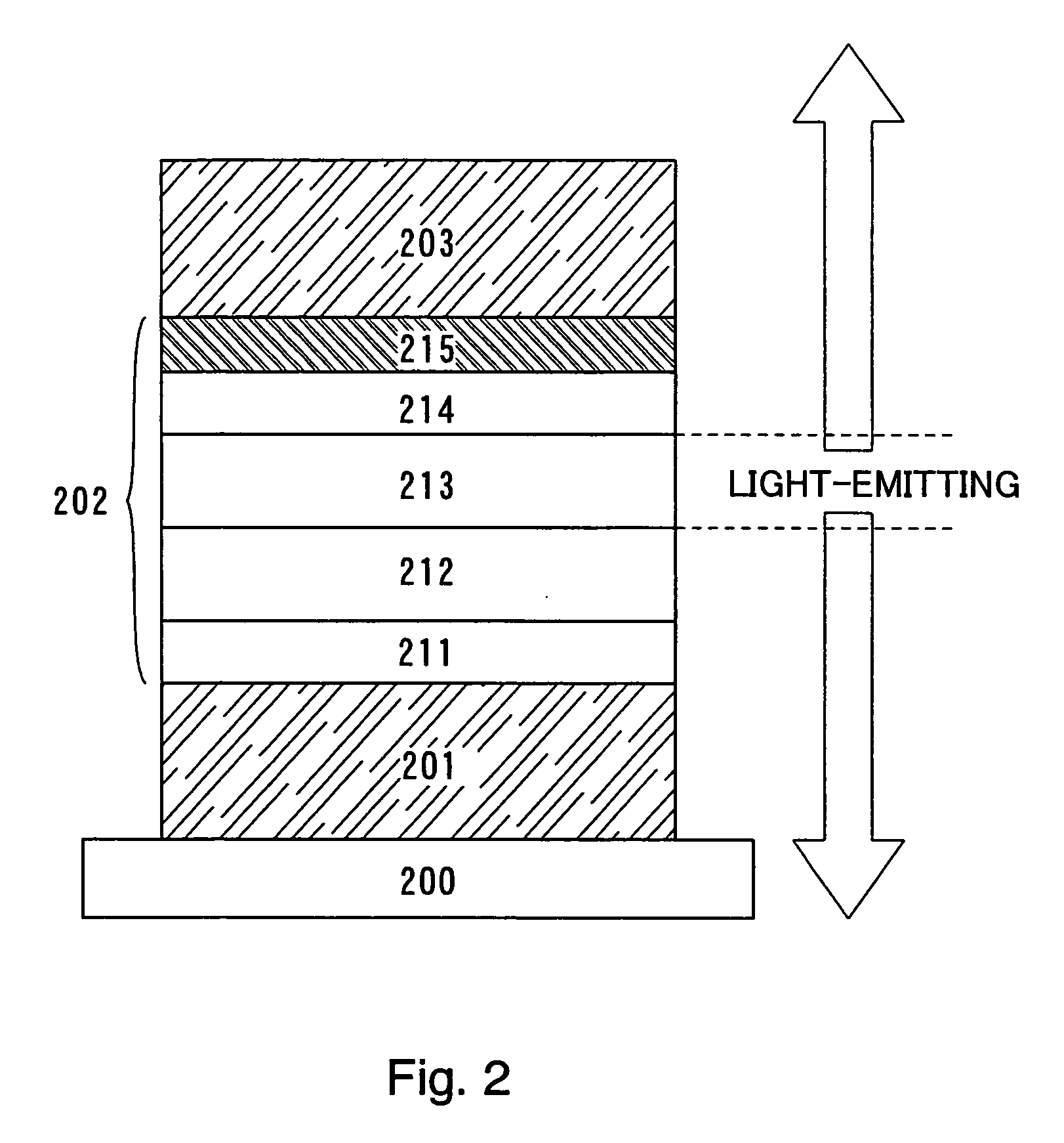
[0050] In the present embodiment, a light-emitting element according to the present invention in the case of a structure in which light generated in a layer including a luminescent material is emitted from both side of first and second electrodes of a light-emitting element (hereinafter, referred to as a both-emission structure), which has an electron injection layer provided in a portion of the layer including the luminescent material, will be described with reference to FIG. 2.
[0051] First, a first electrode 201 of a light-emitting element is formed on a substrate 200. In the present embodiment, the first electrode 201 functions as an anode. ITO that is a transparent conductive film is used as a material to form the first electrode 201 with a film thickness of 110 nm by sputtering.
[0052] Next, a layer 202 including a luminescent material is formed on the first electrode (anode) 201. The layer 202 including the luminescent material in the present embodiment has a laminated struct...
embodiment 2
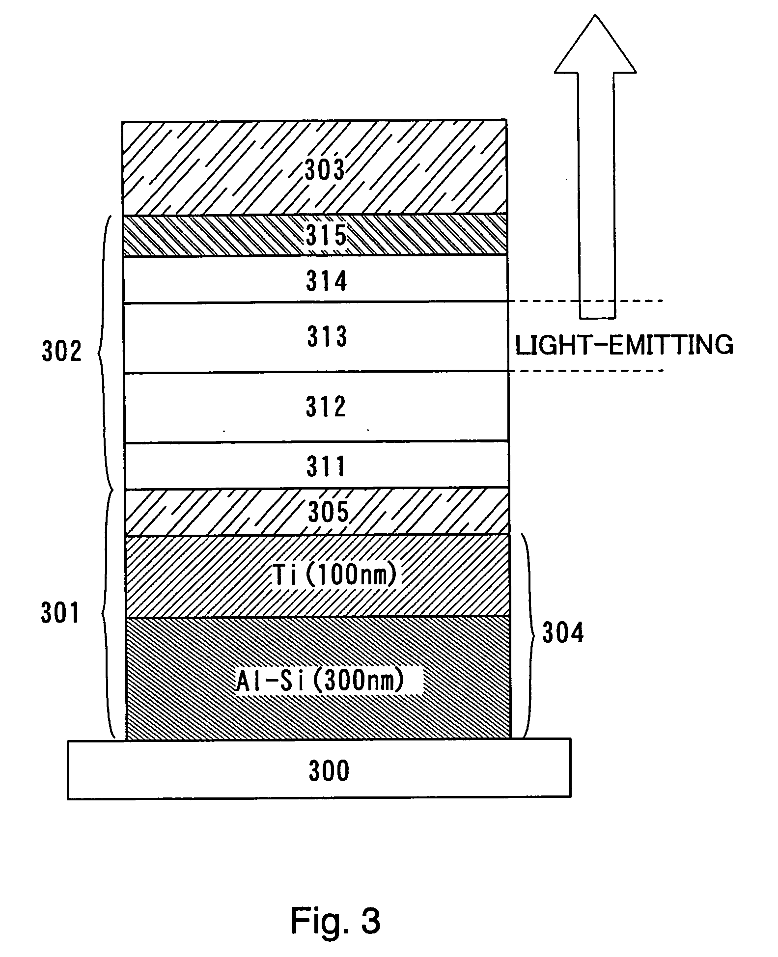
[0062] In the present embodiment, a specific structure in which light is emitted from a second electrode to be formed a layer including a luminescent material (hereinafter, referred to as a top-emission structure) in the case of a structure where light generated in a layer including a luminescent material is emitted from one side of a light-emitting element will be described with reference to FIG. 3.
[0063] Only different portion from the structure in Embodiment 1 will be described here, and descriptions of component parts except a first electrode, which are the same as those of Embodiment 1, will be omitted.
[0064] A first electrode 301 in the present embodiment functions as an anode, from which no light generated in a layer 302 including a luminescent material is emitted. In other words, a nitride or carbide of an element belonging to one of Group 4, Group 5, and Group 6 of the periodic table of the elements, which has a large work function and shields light, such as titanium nitr...
embodiment 3
[0070] In the present invention, a structure in which light is emitted from a side of an electron injection layer 515 included in a layer 502 including a luminescent material as shown in FIG. 4 (hereinafter, referred to as a top-emission structure) can also be employed in the case of a structure where light generated in a layer including a luminescent material is emitted from one side of a light-emitting element as described in Embodiment 2.
[0071] In the same way as Embodiment 2, as a first electrode 501, a reflective conductive film 504 is formed on a substrate 500 and then, a transparent conductive film 505 is formed thereon. After forming the first electrode 501, a hole injection layer 511, a hole transport layer 512, a light-emitting layer 513, an electron transport layer 514, the electron injection layer 515, and a second electrode 503 are sequentially laminated in the same way as Embodiments 1 and 2.
[0072] In the case of the present embodiment, since the second electrode (ca...
PUM
| Property | Measurement | Unit |
|---|---|---|
| work function | aaaaa | aaaaa |
| thickness | aaaaa | aaaaa |
| thickness | aaaaa | aaaaa |
Abstract
Description
Claims
Application Information


