Eureka AIR delivers breakthrough ideas for toughest innovation challenges, trusted by R&D personnel around the world.

Plasma electrode, plasma processing electrode, CVD electrode, plasma CVD device, and method for manufacturing substrate with thin film

Inactive Publication Date: 2016-10-13
TORAY IND INC
View PDF5 Cites 0 Cited by
  • Summary
  • Abstract
  • Description
  • Claims
  • Application Information

AI Technical Summary

Benefits of technology

The invention provides a plasma source that uses less space and has higher productivity compared to conventional technologies. This allows for faster plasma processing and plasma CVD film deposition.

Problems solved by technology

However, there hasn't been any efficient plasma source suggested suitably for a use such as plasma processing and plasma CVD, other than the sputtering film deposition.
When the sputtering electrodes disclosed in Patent documents 1-3 are used for plasma processing or plasma CVD, generated plasma might have different intensities between both sides of cathode or plasma might be generated on one side only, and therefore electric discharge might not be achieved stably and equally on both sides.
Although that may not be a big problem on a sputtering device to form one layer of film on one electric discharge surface, it could cause a poor controllability, on a plasma processing or plasma CVD electrode which generates two kinds of plasma for a single processing.

Method used


Image

  • Plasma electrode, plasma processing electrode, CVD electrode, plasma CVD device, and method for manufacturing substrate with thin film
  • Plasma electrode, plasma processing electrode, CVD electrode, plasma CVD device, and method for manufacturing substrate with thin film
  • Plasma electrode, plasma processing electrode, CVD electrode, plasma CVD device, and method for manufacturing substrate with thin film

Examples


example

[0043]Hereinafter, magnetic circuit analysis results of the plasma electrode described above will be shown as follows.

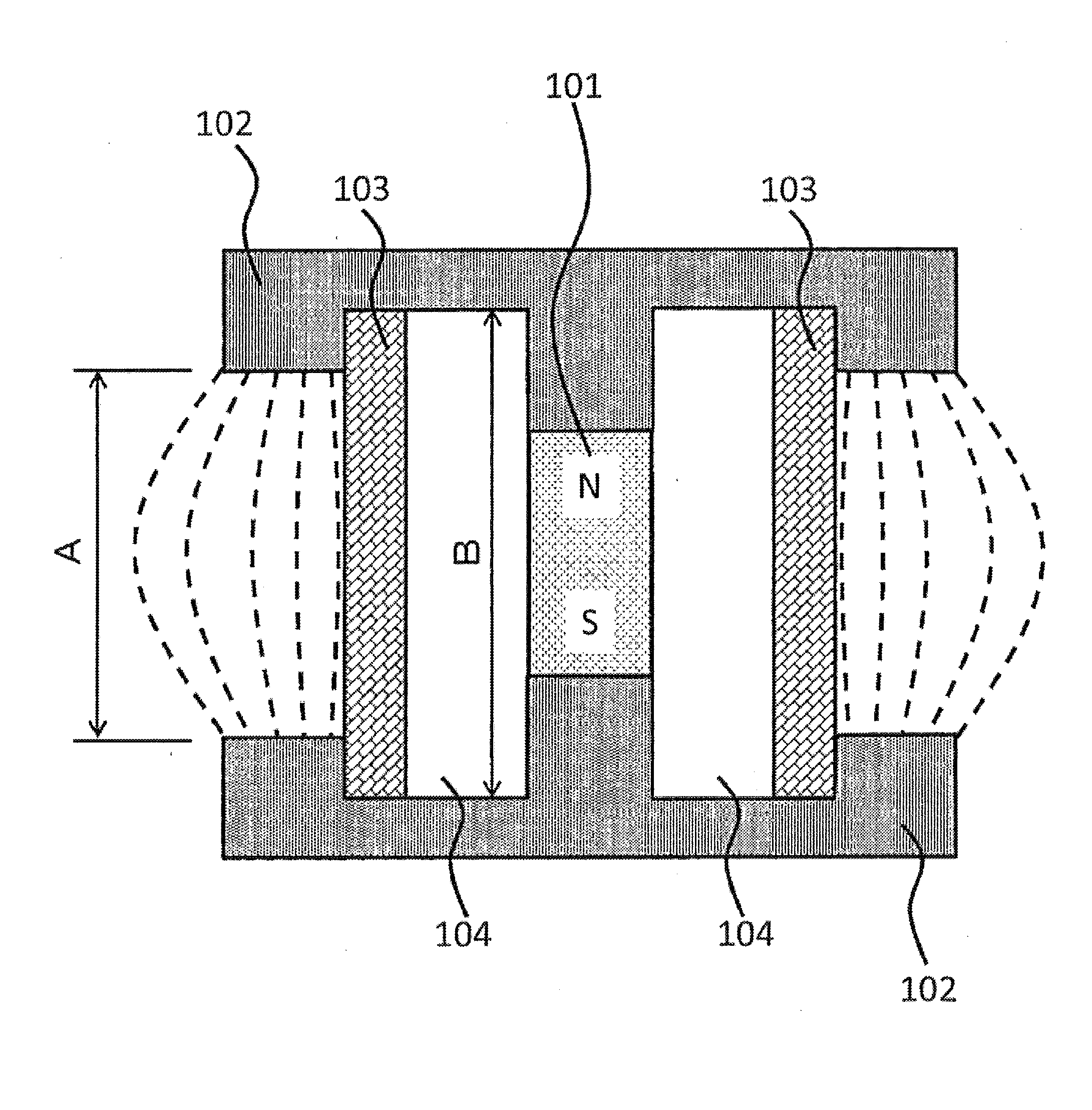
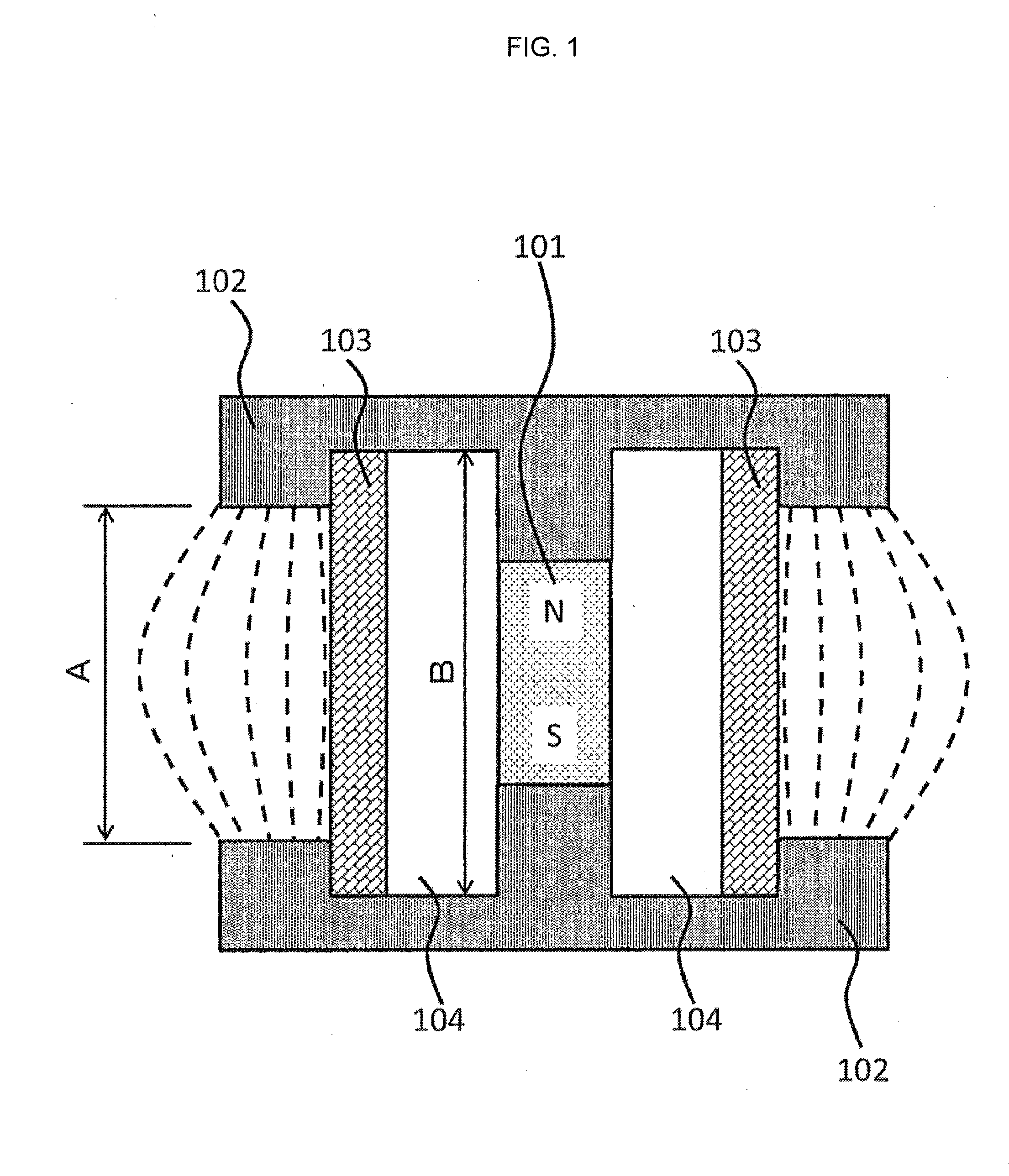
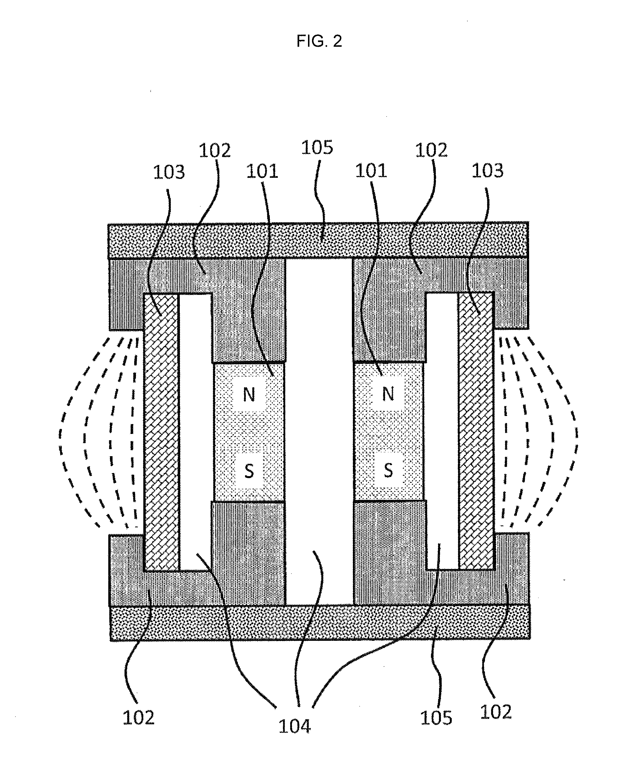
[0044]The main body of electrode shown in FIG. 1 was employed. The analysis was performed under an assumption such that magnet 101 comprises neodymium magnets each having a size of 20 mm in height (in the magnetization direction), 10 mm in width and 40 mm in length and that the magnet surface magnetic flux density is 300 mT. It was also assumed that yoke 102 is made of ferrite-based stainless steel SUS430 and specific magnetic permeability is 500 (absolute magnetic permeability of 1.26×10−6×500 H / m). It is further assumed that cathode 103 is made of pure titanium and coolant water flows in refrigerant flow path 104. The analysis model shown in FIG. 7 was analyzed with STAR-CCM+Ver.7.04.011 under the above-described assumption. The result of analysis showed that a tunnel-shaped magnetic flux is formed to surround a cathode. FIG. 8 and FIG. 9 show the magnetic flux den...


PUM

PropertyMeasurementUnit
Fractionaaaaaaaaaa
Distanceaaaaaaaaaa
Distanceaaaaaaaaaa

Abstract

The present invention relates to a plasma electrode including: an electrode main body having a discharge surface on the outer circumference surface thereof, the interior of the electrode main body having a magnet disposed therein for forming a tunnel-shaped magnetic field on the discharge surface; and ground members which face at least a portion of the discharge surface with a gap therebetween and face each other so as to sandwich the electrode main body therebetween. The discharge surface surrounds the outer circumference of the electrode main body, either with or without a gap interposed therebetween.

Description

CROSS REFERENCE TO RELATED APPLICATIONS[0001]This is the U.S. National Phase application of PCT International Application No. PCT / JP2014 / 079940, filed Nov. 12, 2014, and claims priority to Japanese Patent Application No. 2013-241641, filed Nov. 22, 2013, the disclosures of each of these applications being incorporated herein by reference in their entireties for all purposes.FIELD OF THE INVENTION[0002]Our invention relates to plasma electrode, plasma processing electrode and CVD electrode used for surface treatment and film deposition on the substrate.BACKGROUND OF THE INVENTION[0003]It is generally known that surfaces of substrates can be reformed with plasma and that function film can be formed on the surface of substrates with a film depositing means using plasma. To provide plasma used for these technologies, various plasma electrodes have been developed and put into practical use. From a viewpoint of efficiency, the electrode technology for generating plasma on both sides of an...

Claims


Application Information

Patent Timeline
IPC IPC(8): C23C16/50
CPCC23C16/50H01J37/32532H01J37/34H01J37/3402H05H1/46
Inventor KAWASHITA, MAMORUEJIRI, HIROE
Owner TORAY IND INC
Why Eureka
Eureka Blog
Learn More