Plasma processing method

a processing method and technology of plasma, applied in the field of plasma processing methods, can solve the problems of uneven exposure, unwanted roughness formation on the surface and side walls of the formed circuit pattern of the photoresist, and unnecessary exposure of the photoresist material, so as to reduce the thickness, improve the lithography resolution, and reduce the effect of roughness

Active Publication Date: 2013-07-30
HITACHI HIGH-TECH CORP
View PDF9 Cites 334 Cited by
  • Summary
  • Abstract
  • Description
  • Claims
  • Application Information

AI Technical Summary

Benefits of technology

[0019]Therefore, the present invention aims at providing a plasma processing method, especially for forming gate electrodes of MOS transistors, using a plasma processing apparatus capable of reducing the roughness on the surfaces and side walls of the photoresist film formed in the semiconductor substrate using plasma, and further capable of performing a highly accurate etching process capable of preventing deterioration of semiconductor device performances by reducing the roughness on the sidewalls of the thin films subjected to plasma processing.
[0020]According to the present invention, plasma is generated using gas containing nitrogen elements to subject the photoresist mask pattern to a plasma curing process (a process for stabilizing coating films or resin films by volatilizing solvents or densifying and modifying films is called a curing process, and especially, such process using plasma is called a plasma curing process), by which the roughness on the surfaces and side walls of the photoresist mask pattern is reduced, and thereafter, the laminated thin films disposed below the photoresist mask pattern are subjected to plasma etching process to reduce the roughness on the sides of the formed pattern and to reduce the LER and LWR.
[0021]Further according to the present invention, plasma is generated using gas containing nitrogen elements to initially subject the photoresist mask pattern to a plasma curing process so as to reduce the roughness on the surfaces and side walls of the photoresist mask pattern, and thereafter, a thin film layer disposed directly below the photoresist mask pattern is subjected to plasma etching process, the photoresist mask pattern is subjected again to plasma curing process, a thin film layer disposed below the plasma-processed thin film layer is subjected to plasma etching process, and the photoresist mask pattern and the laminated thin films are alternately respectively subjected to plasma curing process and plasma etching process, by which the roughness on the sides of the laminated thin films is reduced and the LER and LWR are reduced.

Problems solved by technology

In the exposure process of the photolithography technique, ultraviolet rays and the like used for exposing the resist material must reach the bottom of the resist material with sufficient optical intensity, but due to standing waves caused by reflection at the thin film surface or diffused reflection at the stepped portions of the thin film, drawbacks such as exposure of unnecessary portions of the photoresist material and uneven exposure occur.
When the photoresist material is developed, undesirable roughness is formed on the surface and side walls of the formed circuit pattern of the photoresist.
Further, undesirable roughness occurs to the surface and side walls of the resist due for example to uneven resist polymer size, aggregation of polymers having different polarities and uneven oxygen diffusion according to chemical amplification reaction.
As described above, undesirable roughness is formed on the surfaces and side walls of the photoresist circuit pattern formed via a general photolithography technique.
When the photoresist circuit pattern having such roughness is used as the mask to etch laminated thin films disposed below the mask in a plasma etching apparatus, there occurs a drawback in that undesirable roughness is formed on the side walls of the etched thin films similar to the roughness formed on the surfaces and side walls of the photoresist.
However, along with the scaling down of the LSI (large scale integration), the gate length has been reduced to the order of tens of nm, according to which the roughness of a few nm on the side walls of the polysilicon layer transferred via the etching process could not be tolerated, since it affects the performance of the MOS transistor greatly.
Actually, a roughness of a few nm on the side walls of the polysilicon layer causes the gate length of the transistor to be reduced locally in some areas, causing a short channel effect, which leads to the increase of leak current and decrease of threshold voltage.
Moreover, according to the operation properties of multiple transistors, the roughness of a few nm formed on the side walls of the polysilicon layer causes dispersion of gate length, which leads to fluctuation of transistor performances and deterioration of yield.
The problems related to LER and LWR in the process of etching polysilicon electrodes of MOS transistors have been described above, but similar problems exist in processing high-k / metal gate structures and three-dimensional MOSFET, such as FIN-FET, which are considered as the structures of next-generation MOSFET transistors.
However, such improvement in molecular structures causes new drawbacks, such as deterioration of the tolerance of the photoresist mask pattern to plasma etching and insufficient initial film thickness.
The influences of the LER and LWR on the forming of gate electrodes in MOS transistor shave been described as an example, but the problems of LER and LWR occur similarly in the art of hole processing, deep trench processing, STI processing, damascene processing and the like, which have drawbacks in that the circuit pattern cannot be etched with high accuracy and that a semiconductor device with a predetermined performance cannot be manufactured.
Especially, a typical example of the problems of LER and LWR regarding the etching of insulating films using fluorocarbon plasma is the generation of striation caused by plasma damage of the resist mask for ArF exposure.
During such plasma etching having high deposition property and high energy, the surface roughness of the resist mask having been subjected to ArF exposure is increased through etching, and the increased surface roughness is transferred to the insulating film layer or layer to be etched, causing striation.
However, such methods merely suppress the increase of surface roughness of the photoresist layer during etching of the insulating film using fluorocarbon plasma.
The means for suppressing surface roughness in the etching of insulating films are not effective in solving the problems of unnecessary roughness formed on the surface and side walls of the photoresist circuit pattern prior to etching during the processing of gate electrodes.
As described, the problems of LER and LWR caused by unnecessary roughness formed on the surface and side walls of the photoresist circuit pattern prior to etching in the processing of gate electrodes of MOS transistors using fine photoresist circuit patterns have not yet been solved.

Method used


Image

  • Plasma processing method
  • Plasma processing method
  • Plasma processing method

Examples


embodiment 1

[Embodiment 1]

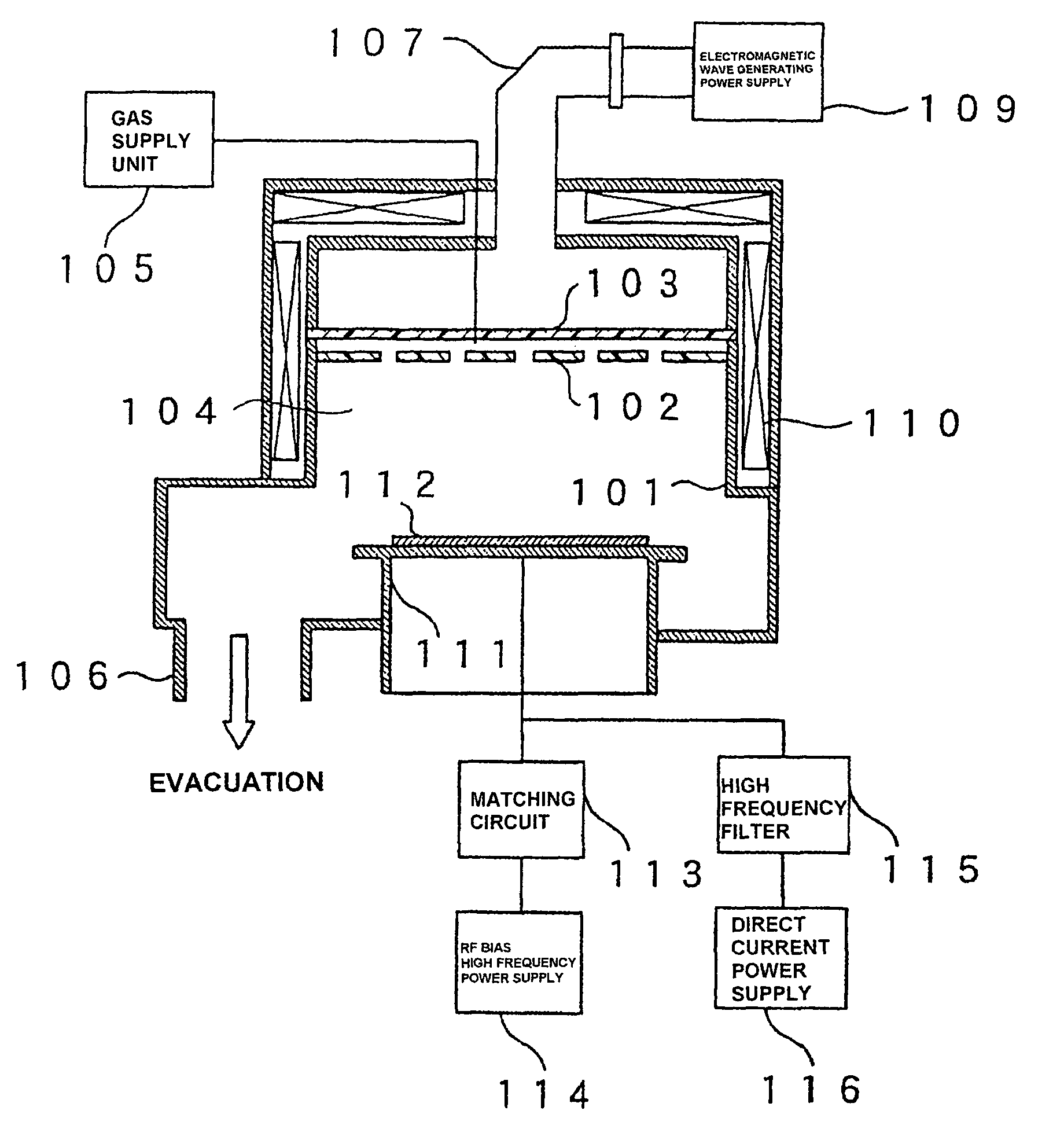
[0051]Next, the plasma processing method for performing etching using plasma according to a first embodiment of the present invention will be described with reference to FIGS. 5 through 8.

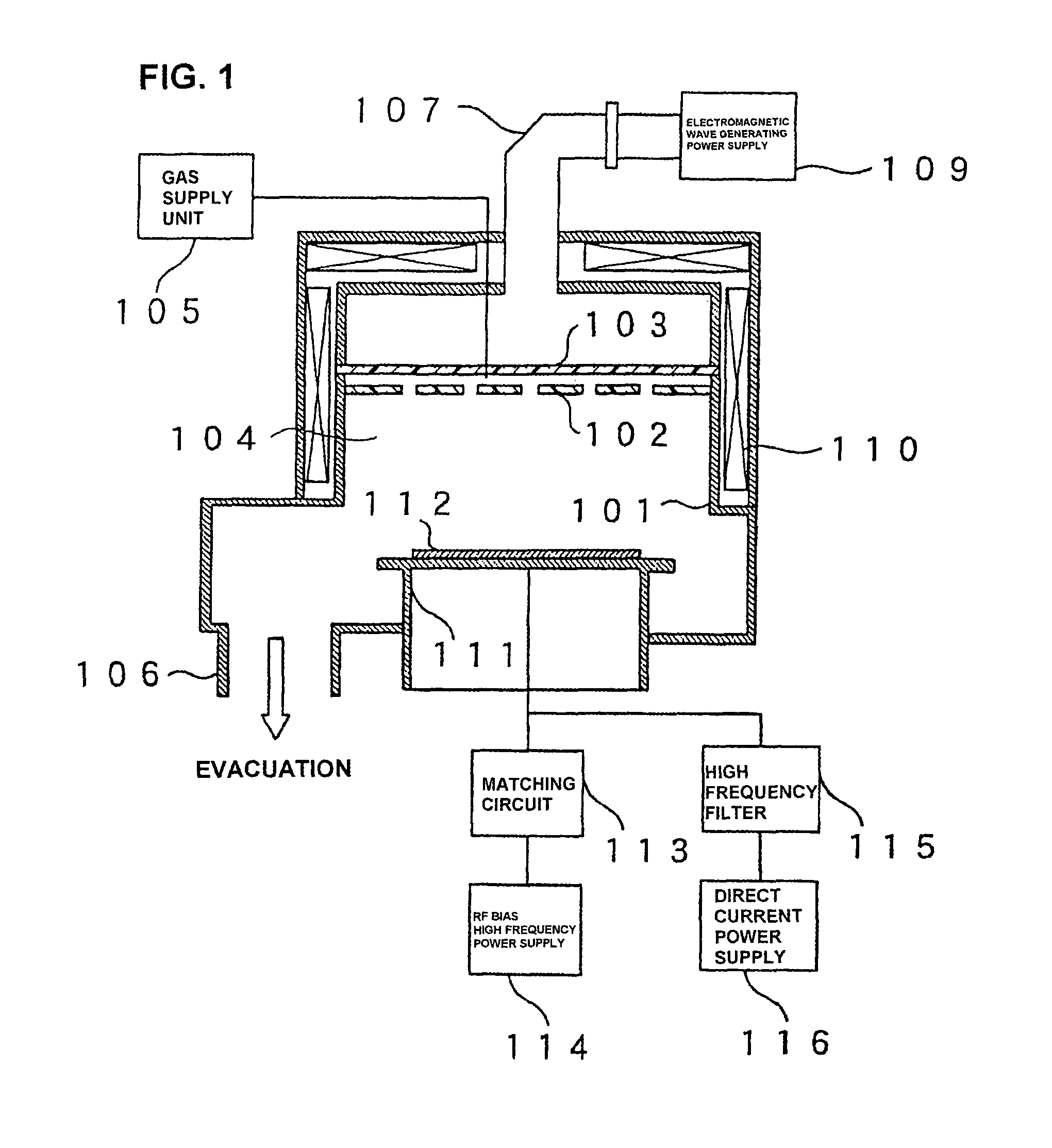
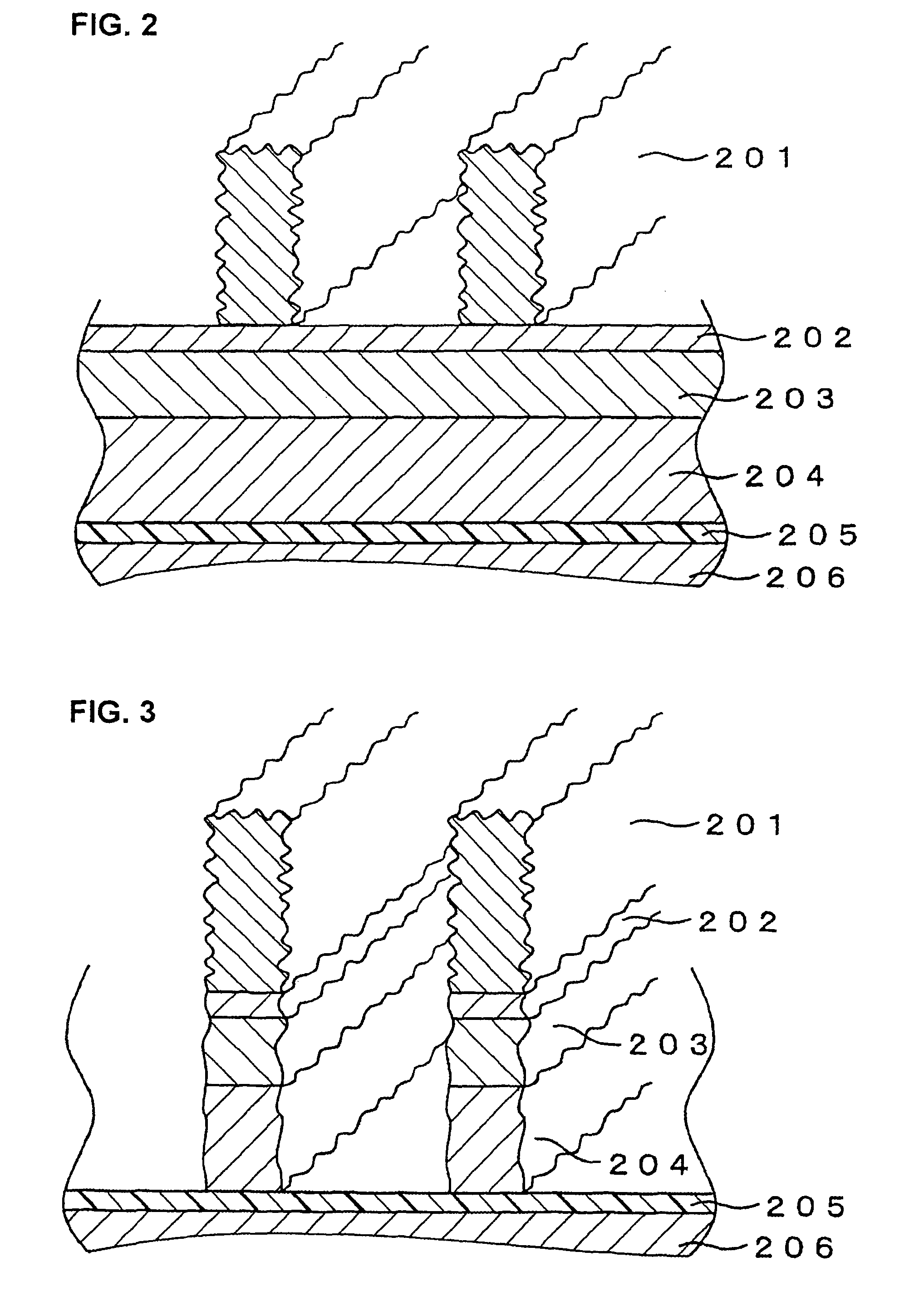
[0052]According to the plasma processing method of the present invention, with respect to the photoresist mask pattern 201 having roughness on the surface and side walls thereof, a plasma curing process is performed to reduce the roughness on the surface and side walls of the photoresist mask pattern 201 as a pretreatment for etching the laminated thin films disposed below the photoresist mask pattern. FIG. 5 illustrates the shape of the material being processed after generating plasma from nitrogen gas and performing a plasma curing process. By performing a plasma curing process, it becomes possible to reduce the roughness on the surface and side walls of the photoresist mask pattern 201 caused by exposure and development of the photoresist material, and therefore, the laminated thin...

embodiment 2

[Embodiment 2]

[0072]A second embodiment of the present invention will now be described with reference to FIG. 10. Only the features that differ from embodiment 1 are described hereafter. FIG. 10 shows a deposition gas flow rate dependency of the LWR and the vertical etching rate of the photoresist material when deposition gas is added to nitrogen gas as the processing gas of the plasma curing process. Heretofore, when a curing process is performed by using only deposition gases, elimination of lactone groups of the photoresist did not occur, and the roughness of the photoresist surface could not be reduced. In the present embodiment, a gas including methane gas diluted by rare gas is used as the deposition gas. When the quantity of the deposition gas being added is increased, the vertical etching rate (1002) of the photoresist material during the plasma curing process is reduced. However, even when the quantity of added deposition gas is increased, the LWR (1001) is not substantiall...


PUM

PropertyMeasurementUnit
RF bias poweraaaaaaaaaa
processing temperatureaaaaaaaaaa

Abstract

The invention provides a method for subjecting laminated thin films disposed below a photoresist mask pattern to plasma processing, wherein the roughness on the side walls of the formed pattern is reduced, and the LER and LWR are reduced. When etching a material to be processed to form a gate electrode including thin films such as a gate insulating film 205, a conducting layer 204, a mask layer 203 and an antireflection film 202 laminated on a semiconductor substrate 206 and a photoresist mask pattern 201 disposed on the antireflection film, prior to etching the mask pattern 201, plasma is generated from nitrogen gas or a mixed gas including nitrogen gas and deposition gas to subject the mask pattern 201 to a plasma curing process so as to reduce the roughness on the surface and side walls of the mask pattern 201, and then the laminated thin films 202, 203 and 204 disposed below the mask pattern 201 are subjected to a plasma etching process.

Description

[0001]The present application is based on and claims priority of Japanese patent application No. 2007-7437 filed on Jan. 16, 2007, the entire contents of which are hereby incorporated by reference.BACKGROUND OF THE INVENTION[0002]1. Field of the Invention[0003]The present invention relates to plasma processing methods, and more specifically, to plasma processing methods suitable for subjecting semiconductor substrates to surface treatments using plasma. The present invention also relates specifically to plasma processing methods suitable for forming gate electrodes in MOS (metal oxide semiconductor) transistors using photolithography.[0004]2. Description of the Related Art[0005]Generally, photolithography techniques are applied in the process of manufacturing semiconductors. Photolithography techniques are composed of the following steps. First, a photoresist material is applied on laminated thin film layers disposed on a semiconductor substrate, which is exposed to ultra violet ray...

Claims


Application Information

Patent Timeline
Patent Type & Authority Patents(United States)
IPC IPC(8): H01L21/302
CPCH01L21/0273H01L21/28035H01L21/32139H01L21/3065
Inventor YASUI, NAOKIWATANABE, SEIICHI
Owner HITACHI HIGH-TECH CORP
Why Eureka
Try Eureka