Plasma processing apparatus and method

a processing apparatus and plasma technology, applied in the direction of electrical apparatus, basic electric elements, electric discharge tubes, etc., can solve the problems of poor plasma resistance properties, etching surface roughness, and formation of vertical lines (striation), and achieve high selectivity etching, effective prevention of deposition, and high rate etching

Active Publication Date: 2011-05-31
TOKYO ELECTRON LTD
View PDF24 Cites 351 Cited by
  • Summary
  • Abstract
  • Description
  • Claims
  • Application Information

AI Technical Summary

Benefits of technology

[0014]The present invention has been made in consideration of the problems described above, and has an object to provide a plasma processing apparatus and plasma processing method, which can realize high selectivity etching while maintaining the plasma resistance properties of a resist layer or organic mask layer at a high level, or can effectively prevent deposition on an electrode, or can realize high rate etching, or can realize uniform etching on a target substrate.

Problems solved by technology

However, since the ArF photo-resist has poor plasma resistance properties, its surface becomes rough during etching, which is scarcely caused in the KrF resist.
Accordingly, problems arise in that vertical lines (striation) are formed on the inner wall of opening portions, or opening portions are expanded (increase in CD).
Furthermore, in parallel-plate etching apparatuses of the capacitive coupling type, where the pressure in the chamber is high and the etching gas in use is a negative gas (for example, CxFy or O2), the plasma density becomes low at the chamber central portion, which makes it difficult to control the plasma density.

Method used


Image

  • Plasma processing apparatus and method
  • Plasma processing apparatus and method
  • Plasma processing apparatus and method

Examples


Embodiment Construction

[0068]Embodiments of the present invention will be described hereinafter with reference to the accompanying drawings.

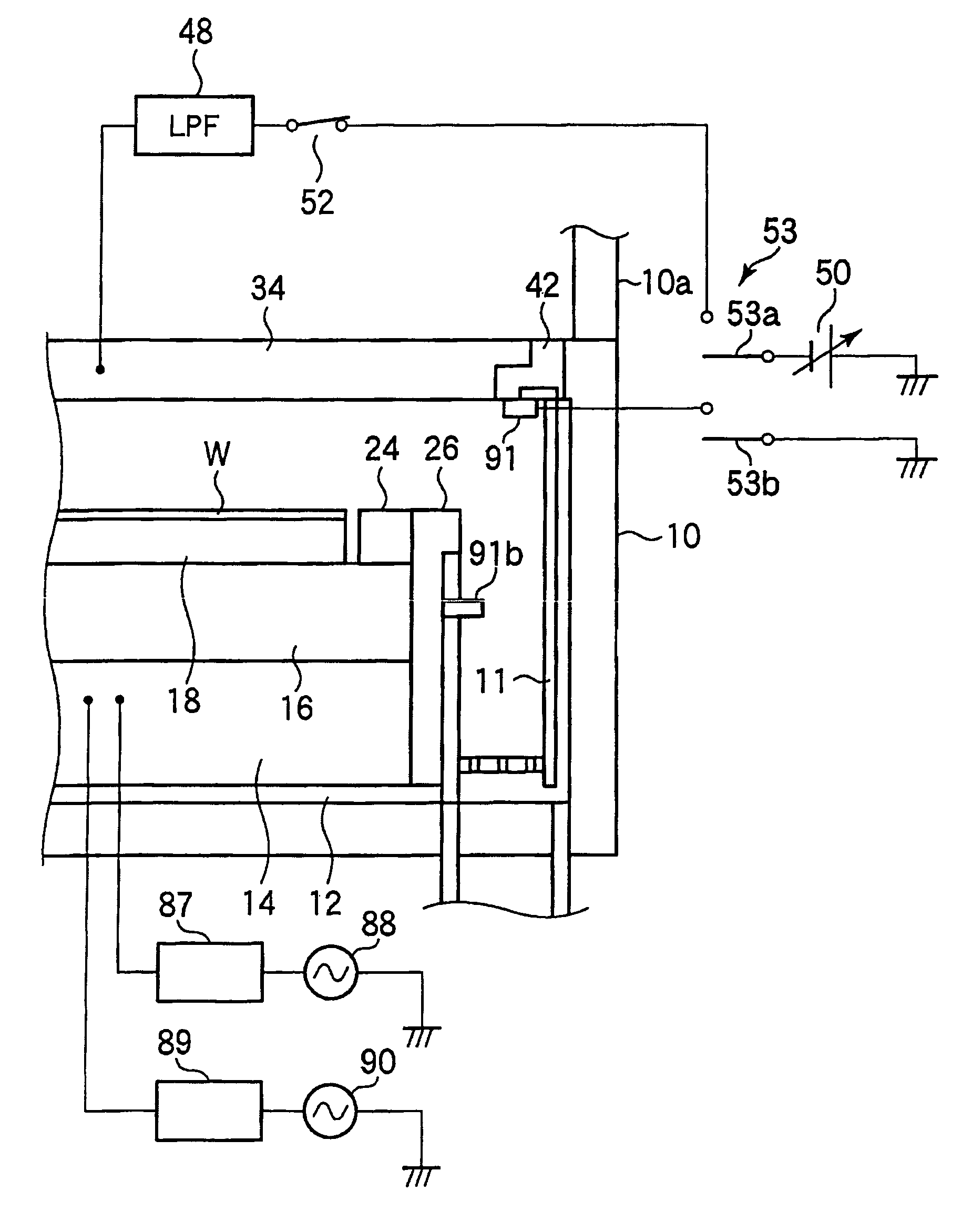
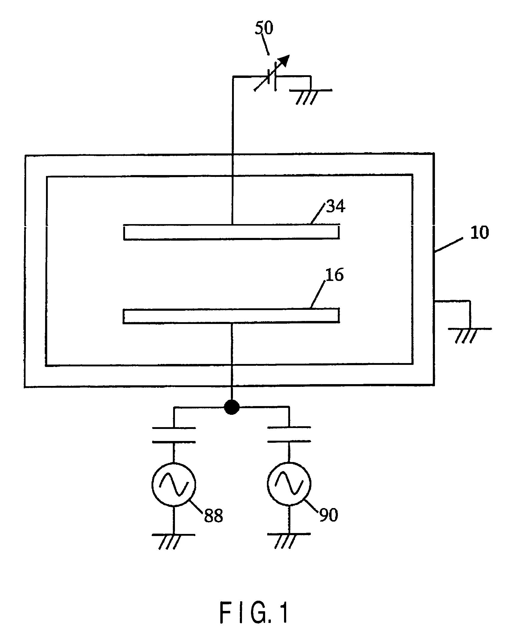
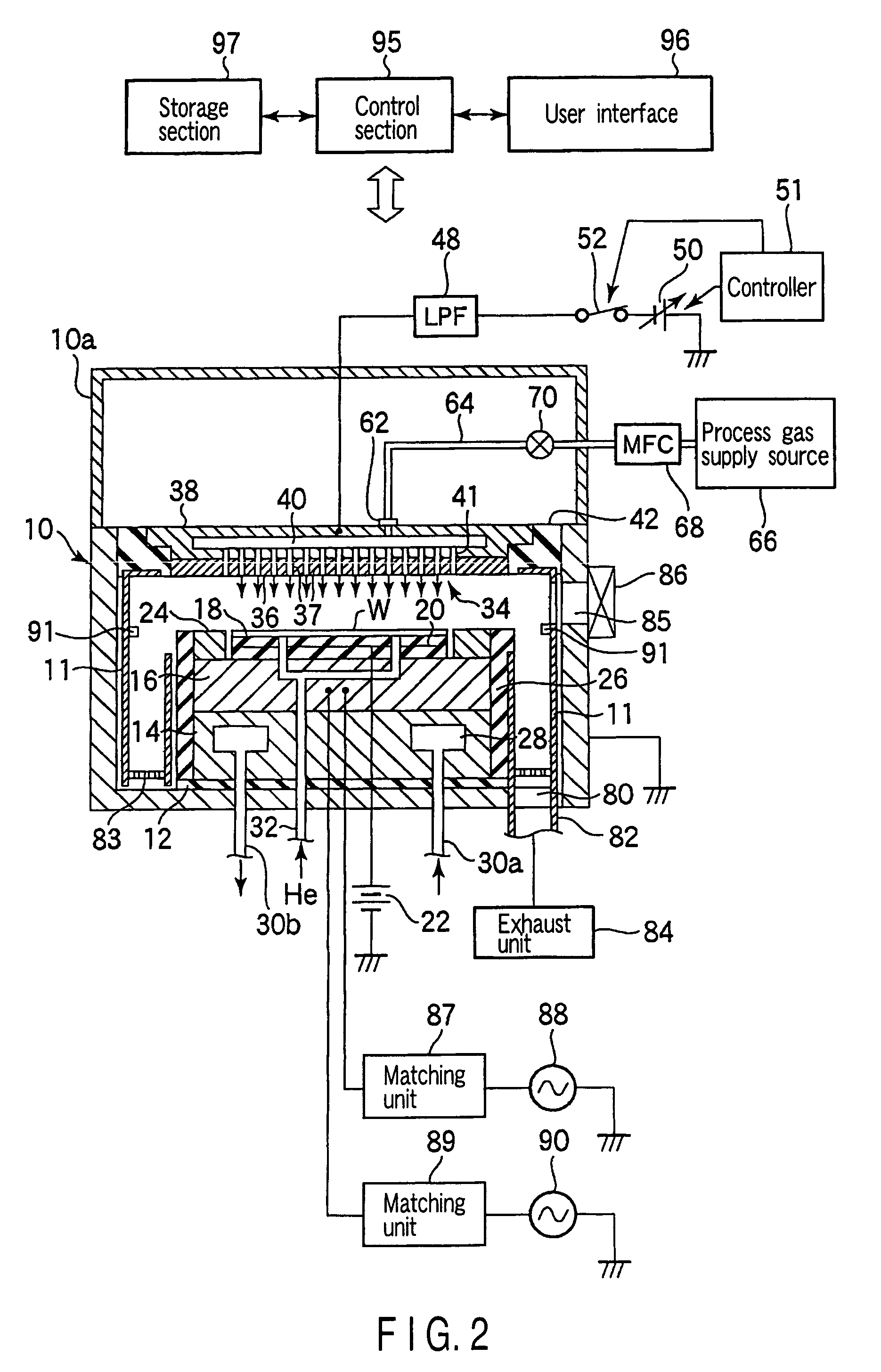
[0069]FIG. 1 is a sectional view schematically showing a plasma etching apparatus according to an embodiment of the present invention.

[0070]This plasma etching apparatus is of the type that applies two RF powers with different frequencies to the lower side. Specifically, a radio frequency (RF) power with, e.g., 40 MHz for plasma generation from a first RF power supply 88 and a radio frequency (RF) with, e.g., 2 MHz for ion attraction from a second RF power supply 90 are applied to a lower electrode or susceptor 16. Further, as shown in FIG. 1, a variable DC power supply 50 is connected to an upper electrode 34 to apply a predetermined direct current (DC) voltage. With reference to FIG. 2, this plasma etching apparatus will be explained in more detail.

[0071]This plasma etching apparatus is structured as a parallel-plate plasma etching apparatus of the capacitive coupli...


PUM

PropertyMeasurementUnit
frequencyaaaaaaaaaa
frequencyaaaaaaaaaa
frequencyaaaaaaaaaa

Abstract

An apparatus includes an upper electrode and a lower electrode for supporting a wafer disposed opposite each other within a process chamber. A first RF power supply configured to apply a first RF power having a relatively higher frequency, and a second RF power supply configured to apply a second RF power having a relatively lower frequency is connected to the lower electrode. A variable DC power supply is connected to the upper electrode. A process gas is supplied into the process chamber to generate plasma of the process gas so as to perform plasma etching.

Description

CROSS-REFERENCE TO RELATED APPLICATIONS[0001]This application claims the benefit of U.S. Provisional Applications No. 60 / 589,831, filed Jul. 22, 2004; No. 60 / 650,957, filed Feb. 9, 2005; and No. 60 / 662,344, filed Mar. 17, 2005.[0002]This application is based upon and claims the benefit of priority from the prior Japanese Patent Applications No. 2004-183093, filed Jun. 21, 2004; No. 2005-013912, filed Jan. 21, 2005; and No. 2005-045095, filed Feb. 22, 2005, the entire contents of all of which are incorporated herein by reference.BACKGROUND OF THE INVENTION[0003]1. Field of the Invention[0004]The present invention relate to a plasma processing apparatus, plasma processing method, and computer readable storage medium, used for performing a plasma process on a target substrate, such as a semiconductor substrate.[0005]2. Description of the Related Art[0006]For example, in manufacturing semiconductor devices, plasma etching processes, which utilize plasma to etch a layer through a resist ...

Claims


Application Information

Patent Timeline
Patent Type & Authority Patents(United States)
IPC IPC(8): C23F1/00H01L21/306
CPCH01J37/32082H01L21/3065H01J37/32706H01J37/32174H01J37/32091H01J37/3244H01J37/32697H01J2237/334
Inventor KOSHIISHI, AKIRASUGIMOTO, MASARUHINATA, KUNIHIKOKOBAYASHI, NORIYUKIKOSHIMIZU, CHISHIOOHTANI, RYUJIKIBI, KAZUOSAITO, MASASHIMATSUMOTO, NAOKIIWATA, MANABUYANO, DAISUKEYAMAZAWA, YOHEIHANAOKA, HIDETOSHIHAYAMI, TOSHIHIROYAMAZAKI, HIROKISATO, MANABU
Owner TOKYO ELECTRON LTD
Why Eureka
Try Eureka