High-permittivity insulation film, thin film capacity element, thin film multilayer capacitor, and production method of thin film capacity element

a technology of high-permittivity insulation and capacity elements, which is applied in the direction of stacked capacitors, fixed capacitor details, fixed capacitors, etc., can solve the problems of deterioration of leakage properties and breakdown voltages, poor surface smoothness of dielectric films to be formed, and decrease of permittivity, so as to achieve enhanced effect of present invention and improve leakage properties

Active Publication Date: 2006-05-04
TDK CORPARATION
View PDF5 Cites 21 Cited by
  • Summary
  • Abstract
  • Description
  • Claims
  • Application Information

AI Technical Summary

Benefits of technology

[0036] In the present invention, “m” in the composition formula is not particularly limited but it is preferably any one of 3, 4 and 5. When in a composition of m=3, 4 or 5, effects of the present invention are particularly enhanced.
[0037] In the present invention, the first bismuth layer-structured compo

Problems solved by technology

For example, a thin film capacitor using a single-layer dielectric thin film is behind in making a compact integrated circuit with a transistor or other active element, which has been a factor of hindering realization of an ultra-high integrated circuit.
Also, in recent years, a conventional multilayer film of SiO2 and Si3N4 has become hard to respond to a capacitor material for a DRAM of the next generation (gigabit generation) in terms of capacity density, and a material system having a higher permittivity has gathered attention.
However, when using dielectric materials of this kind, the permittivity declined as the dielectric film became thinner in some cases.
Also, a leakage property and a breakdown voltage were deteriorated due to apertures generated on the dielectric film as the film became thinner in some cases.
Furthermore, it was liable that the dielectric film to be formed had poor surface smoothness and a permittivity change rate against a temperature was deteriorated.
However, for example, when producing a multilayer ceramic capacitor by a sheet method (a method of forming a dielectric green sheet layer on a carrier film by using a dielectric layer paste by the doctor blade method, etc., printing an internal electrode layer paste to be a predetermined pattern thereon, then, releasing them one by one and stacking the same), the dielectric layer could not be made thinner than

Method used


Image

  • High-permittivity insulation film, thin film capacity element, thin film multilayer capacitor, and production method of thin film capacity element
  • High-permittivity insulation film, thin film capacity element, thin film multilayer capacitor, and production method of thin film capacity element
  • High-permittivity insulation film, thin film capacity element, thin film multilayer capacitor, and production method of thin film capacity element

Examples


first embodiment

[0062] In the present invention, a thin film capacitor, wherein a dielectric thin film is formed by a single layer, will be explained as an example of a thin film capacity element.

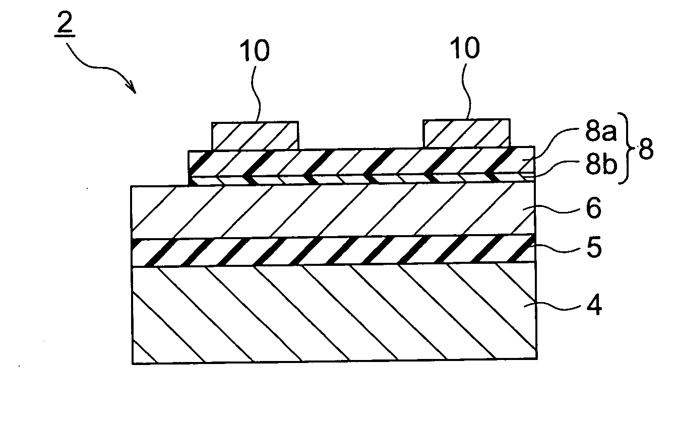
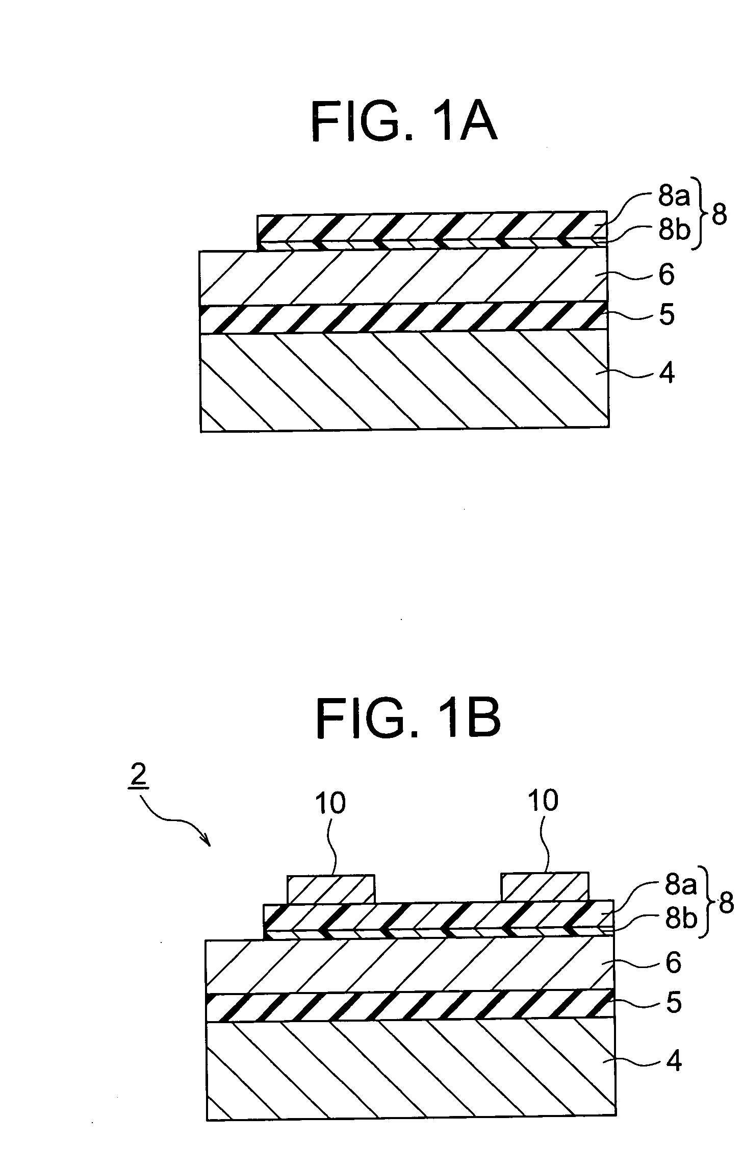
[0063] As shown in FIG. 1A, a thin film capacitor 2 according to an embodiment of the present invention has a substrate 4, and a lower portion electrode thin film 6 is formed on the substrate 4 via an insulation layer 5. A dielectric thin film (high-permittivity insulation film) 8 is formed on the lower portion electrode thin film 6. As shown in FIG. 1B, an upper portion electrode thin film 10 is formed on the dielectric thin film 8.

[0064] The substrate 4 is not particularly limited but composed of a single crystal having good lattice matching (for example, SrTiO3 single crystal, MgO single crystal and LaAlO3 single crystal, etc.), an amorphous material (for example, glass, fused silica and SiO2 / Si, etc.) and other material (for example, ZrO2 / Si and CeO2 / Si, etc.), etc. A thickness of the substrate 4 is ...

second embodiment

[0109] In the present embodiment, a thin film multilayer capacitor, wherein the dielectric thin film is formed by multilayer, will be explained as an example of a thin film capacity element.

[0110] As shown in FIG. 3, a thin film multilayer capacitor 20 according to an embodiment of the present invention has a capacitor element 22. The capacitor element 22 has a multilayer structure, wherein a plurality of dielectric thin films 80 and internal electrode thin films 24 and 26 are alternately arranged on a substrate 4a and a protective layer 30 is formed to cover the outermost arranged dielectric thin film 80. At both end portions of the capacitor element 22 are formed with a pair of external electrodes 28 and 29, and the pair of external electrodes 28 and 29 are electrically connected to exposed end surfaces of the plurality of internal electrode thin films 24 and 26 alternately arranged in the capacitor element 22 so as to configure a capacitor circuit. A shape of the capacitor eleme...

example 1

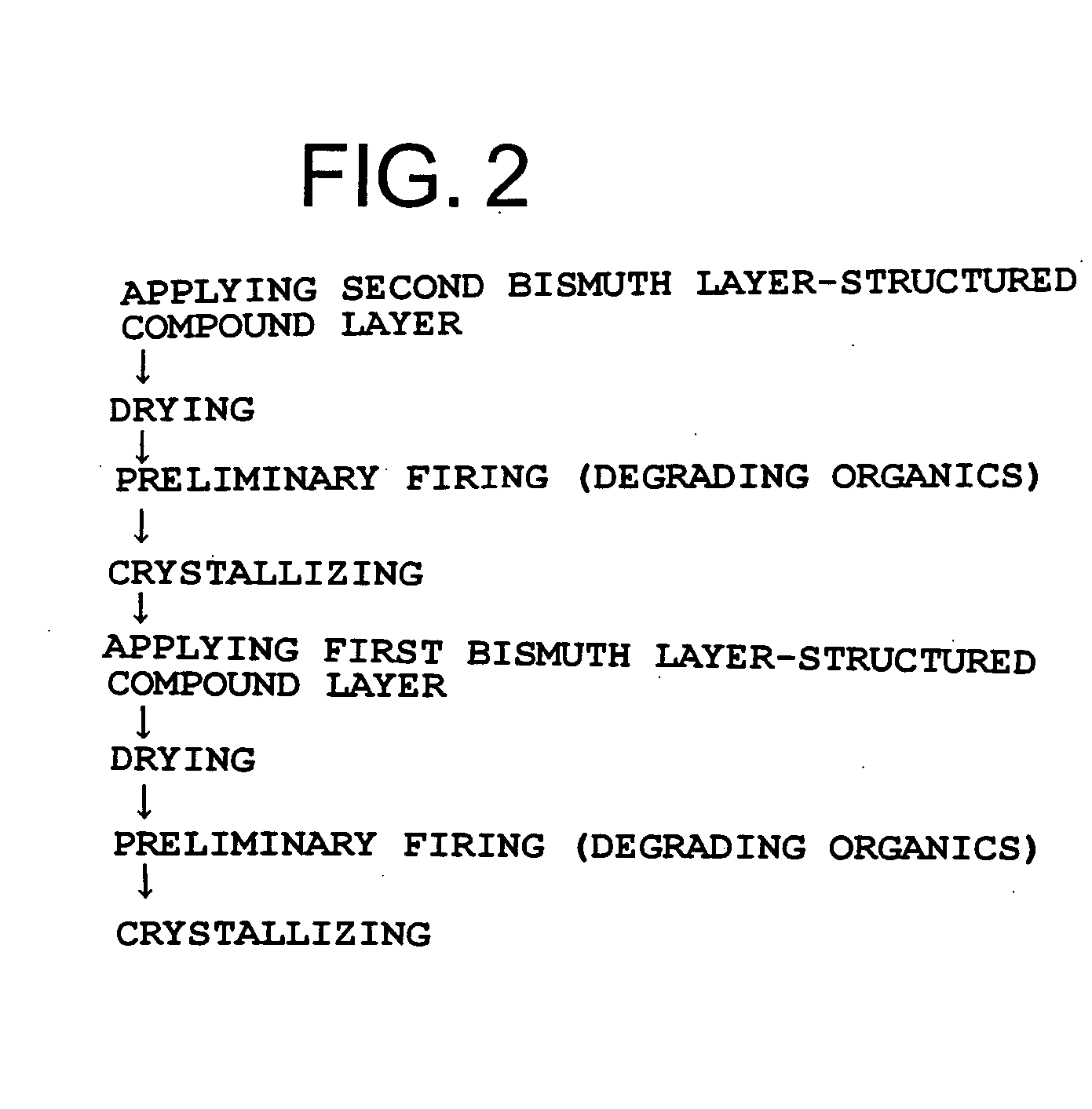
[0118] As shown in FIG. 2, a material solution for forming the second bismuth layer-structured compound layer 8b shown in FIG. 1 was fabricated first. In the present example, to compose the second bismuth layer-structured compound layer 8b by a bismuth layer-structured compound expressed by a composition formula of Bi4+αTi3O12 including bismuth in excess of that in a bismuth layer-structured compound expressed by a stoichiometric composition of Bi4Ti3O12 (BiT) and a composition formula of Bi2Am−1BmO3m+3, wherein m=3, A2=Bi2 and B3=Ti3, a solution below was prepared.

[0119] First, a 2-ethylhexanoate solution of 2-ethylhexanoate Bi, and a toluene solution of 2-ethylhexanoate Ti were prepared as material solutions. Namely, the two solutions were mixed, so that the Bi adding quantity was increased by α mole comparing with that in the case of mixing them at the stoichiometric ratio, such as (4+α) moles of 2-ethyl hexanoate Bi and 3 moles of 2-ethyl hexanoate Ti, and the result was dilute...


PUM

PropertyMeasurementUnit
Temperatureaaaaaaaaaa
Fractionaaaaaaaaaa
Thicknessaaaaaaaaaa

Abstract

A dielectric thin film 8, comprising a first bismuth layer-structured compound layer 8a expressed by a composition formula of (Bi2O2)2+(Am−1 Bm O3m+1)2− or Bi2 Am−1 Bm O3m+3, wherein “m” is a positive number, “A” is at least one element selected from Na, K, Pb, Ba, Sr, Ca and Bi, and “B” is at least one element selected from Fe, Co, Cr, Ga, Ti, Nb, Ta, Sb, V, Mo and W. Between the first bismuth layer-structured compound layer 8a and a lower portion electrode 6, a second bismuth layer-structured compound layer 8b including bismuth in excess of that in the composition formula of said first bismuth layer-structured compound layer 8a.

Description

TECHNICAL FIELD [0001] The present invention relates to a high-permittivity insulation film, a thin film capacity element, a thin film multilayer capacitor and a production method of the thin film multilayer capacitor. BACKGOUND ART [0002] In recent years, in the field of electronic devices, there have been demands for a furthermore compact capacitor element as an essential circuit element in a variety of electronic circuits along with electronic circuits becoming higher in density and more highly integrated. [0003] For example, a thin film capacitor using a single-layer dielectric thin film is behind in making a compact integrated circuit with a transistor or other active element, which has been a factor of hindering realization of an ultra-high integrated circuit. It was a low permittivity of a dielectric material to be used that has hindered attaining of a compact thin film capacitor. Accordingly, it is significant to use a dielectric material having a high permittivity to realiz...

Claims


Application Information

Patent Timeline
IPC IPC(8): H01L29/00H01L21/00C01G29/00C04B35/475H01G4/12H01G4/30H01L21/02
CPCC01G29/006C01P2006/40C04B35/475C04B2235/3213C04B2235/6585C04B2235/787H01G4/1218H01G4/30H01L28/55Y10S438/957H01G4/33
Inventor MIYAMOTO, YUKISAKASHITA, YUKIO
Owner TDK CORPARATION
Why Eureka
Try Eureka