Bias-boosting circuit with a modified wilson current mirror circuit for radio frequency power amplifiers

a power amplifier and bias-boosting technology, applied in the field of radio frequency integrated circuits, can solve the problems of power amplifiers that may exhibit gain compression at high signal levels, typical transceivers that do not generate enough power or have sufficient sensitivity in itself for reliable communication, etc., to achieve the effect of reducing the footprint of semiconductor dies, extending the 1 db compression point, and reducing cos

Inactive Publication Date: 2016-10-20
MORFIS SEMICON
View PDF0 Cites 13 Cited by
  • Summary
  • Abstract
  • Description
  • Claims
  • Application Information

AI Technical Summary

Benefits of technology

[0011]The present disclosure is directed to a modified Wilson current mirror circuit that provides a bias boost for power amplifier transistors. In accordance with various embodiments, a balance between power amplifier efficiency and linearity is maintained, while extending its 1 dB compression point. For the same output power, a relatively smaller transistor or amplifier circuit can be employed, leading to a reduced semiconductor die footprint as well as lower cost.

Problems solved by technology

Typical transceivers do not generate sufficient power or have sufficient sensitivity in itself for reliable communications.
In particular, such power amplifiers may exhibit gain compression at high signal levels because of a voltage drop (I*R) across bipolar transistors, or because of a fixed voltage bias in field effect transistors.

Method used


Image

  • Bias-boosting circuit with a modified wilson current mirror circuit for radio frequency power amplifiers
  • Bias-boosting circuit with a modified wilson current mirror circuit for radio frequency power amplifiers
  • Bias-boosting circuit with a modified wilson current mirror circuit for radio frequency power amplifiers

Examples


Embodiment Construction

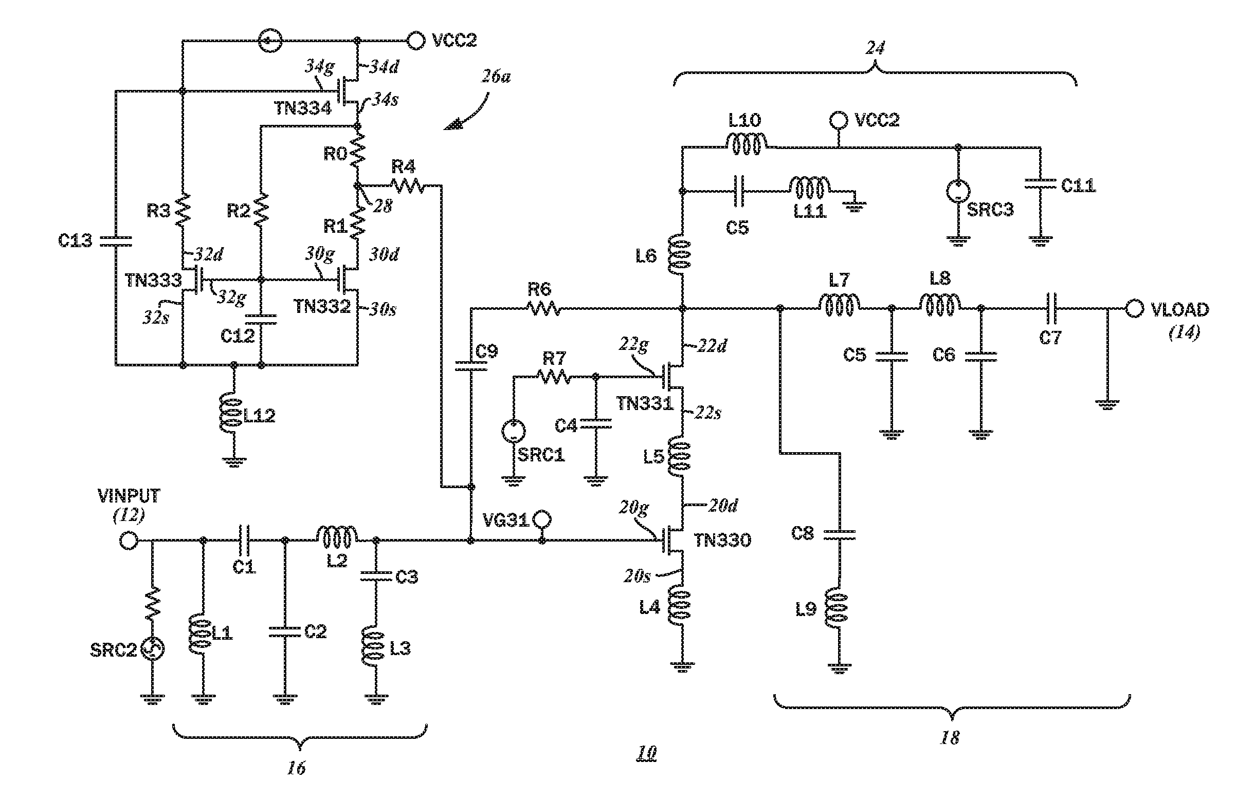
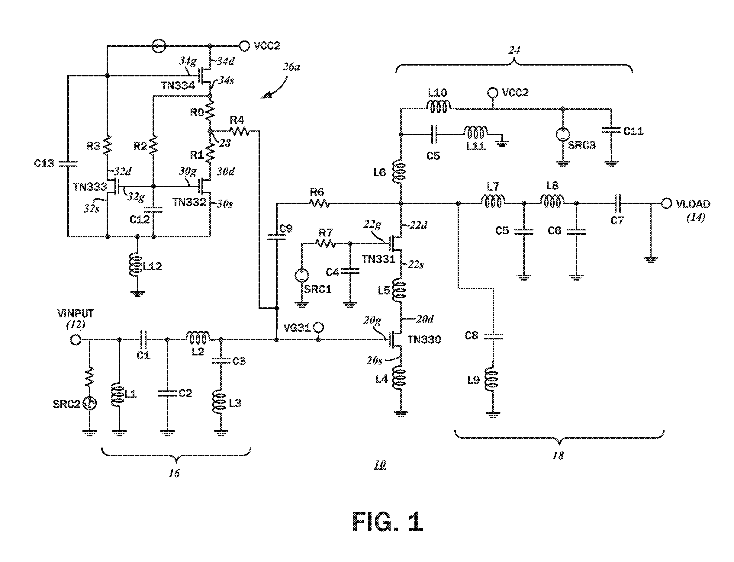
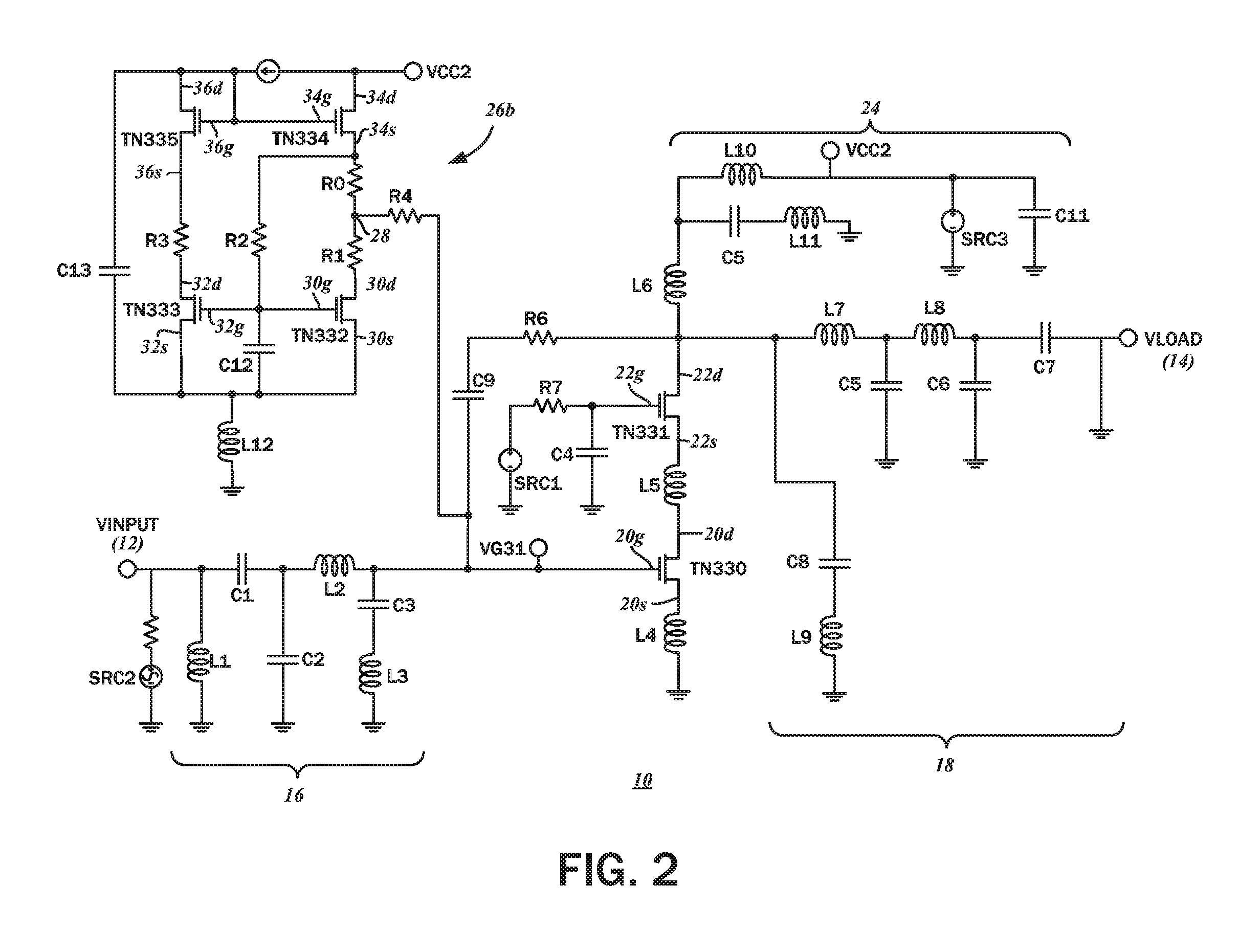
[0021]The detailed description set forth below in connection with the appended drawings is intended as a description of the several presently contemplated embodiments of a modified Wilson current mirror circuit for RF power amplifiers, and is not intended to represent the only form in which the disclosed invention may be developed or utilized. The description sets forth the functions and features in connection with the illustrated embodiments. It is to be understood, however, that the same or equivalent functions may be accomplished by different embodiments that are also intended to be encompassed within the scope of the present disclosure. It is further understood that the use of relational terms such as first and second and the like are used solely to distinguish one from another entity without necessarily requiring or implying any actual such relationship or order between such entities.

[0022]Referring to the schematic diagram of FIG. 1, one embodiment of the present disclosure is...


PUM


Abstract

A current mirror circuit for biasing a power amplifier includes a modified Wilson current mirror with a pair of first and second mirror transistors connected to a third transistor. The first mirror transistor is configured for operating in a saturation mode, with a gate voltage of the first mirror transistor being lower than a gate voltage of the power amplifier. The third transistor charges the power amplifier circuit during a positive half cycle of an input signal and the first mirror transistor discharges the power amplifier circuit during a negative half cycle of the input signal at different rates.

Description

CROSS-REFERENCE TO RELATED APPLICATIONS[0001]This application relates to and claims the benefit of U.S. Provisional Application No. 62 / 148,677, filed Apr. 16, 2015 and entitled “BIAS-BOOSTING CIRCUIT WITH A MODIFIED WILSON CURRENT MIRROR CIRCUIT FOR RF POWER AMPLIFIER” the entirety of the disclosure of which is wholly incorporated by reference herein.STATEMENT RE: FEDERALLY SPONSORED RESEARCH / DEVELOPMENT[0002]Not ApplicableBACKGROUND[0003]1. Technical Field[0004]The present disclosure relates generally to radio frequency (RF) integrated circuits, and more particularly, to a bias-boosting circuit with a modified Wilson current mirror circuit for RF power amplifiers.[0005]2. Related Art[0006]Wireless communications systems find applications in numerous contexts involving information transfer over long and short distances alike, and there exists a wide range of modalities suited to meet the particular needs of each. Generally, wireless communications involve an RF carrier signal that i...

Claims


Application Information

Patent Timeline
Patent Type & Authority Applications(United States)
IPC IPC(8): H03F3/213H03F1/02H03F3/195
CPCH03F3/213H03F3/195H03F2200/18H03F2200/451H03F1/0205H03F1/0261H03F1/223H03F1/3205H03F3/245
Inventor LUO, SIFENXU, ZHANCHEN, CHANGLILI, HAITAOCHANG, HENG-CHIAWANG, NARISIYOON, JUNG HO
Owner MORFIS SEMICON
Why Eureka
Try Eureka