OLED Pixel Compensation Circuit

Active Publication Date: 2016-10-27
EVERDISPLAY OPTRONICS (SHANGHAI) CO LTD
View PDF3 Cites 12 Cited by
  • Summary
  • Abstract
  • Description
  • Claims
  • Application Information

AI Technical Summary

Benefits of technology

[0027]In the OLED pixel compensation circuit according to the present invention, since electrical leakage occurs in the fourth and fifth transistors or the ninth transistor of the initialization module in the off state, the gate voltage of the driving transistor is reduced. The gate voltage of the driving transistor is compensated by the second transistor to assure the stability of the gate voltage of the driving transistor. This reduces the influence on the gate voltage of the driving

Problems solved by technology

Despite the above advantages, OLED display devices incur many problems during applications.
If the gate voltage is unstable, the brightness of the black state is affected and results in a reduction in the contrast ratio and an increase in the value of the storage capacitor.
Thus, the space occupied by the storage capacitor is increased, the output space

Method used


Image

  • OLED Pixel Compensation Circuit
  • OLED Pixel Compensation Circuit
  • OLED Pixel Compensation Circuit

Examples


first embodiment

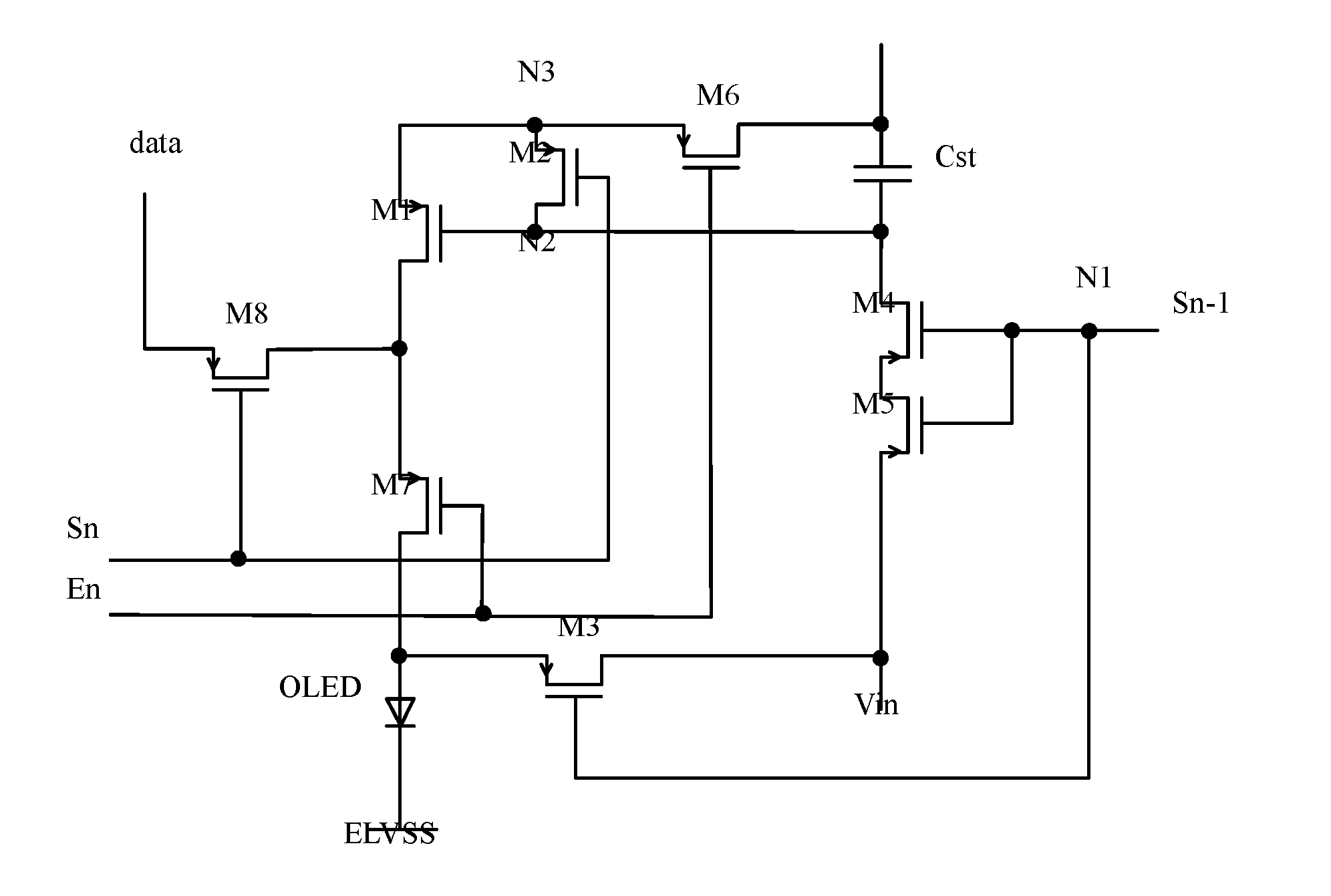
[0090]FIG. 3 is a circuit diagram of the first embodiment of the OLED pixel compensation circuit according to the present invention.

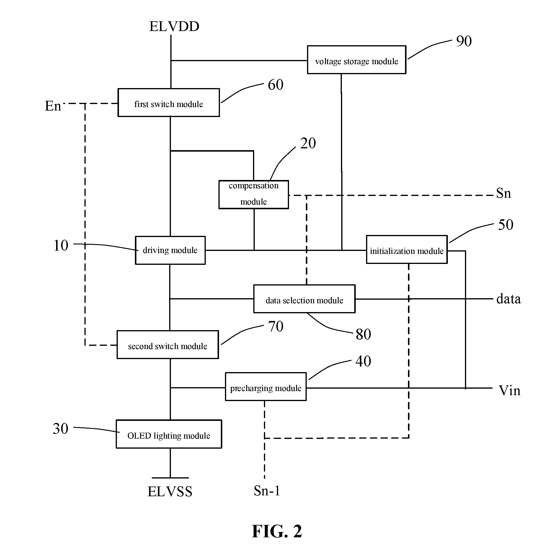
[0091]Specifically, the driving module 10 includes a driving transistor M1. The driving transistor M1 includes a first electrode connected to the second terminal of the first switch module 60. The driving transistor M1 further includes a second electrode connected to the first terminal of the second switch module 70. The driving transistor M1 further includes a gate connected to the second terminal of the compensation module 20, the first terminal of the initialization module 50, and the second terminal of the voltage storage module 90. The first electrode of the driving transistor M1 serves as the first terminal of the driving module 10. The second electrode of the driving transistor M1 serves as the second terminal of the driving module 10. The gate of the driving transistor M1 serves as the control terminal of the driving module 10.

[0092]The compensa...

second embodiment

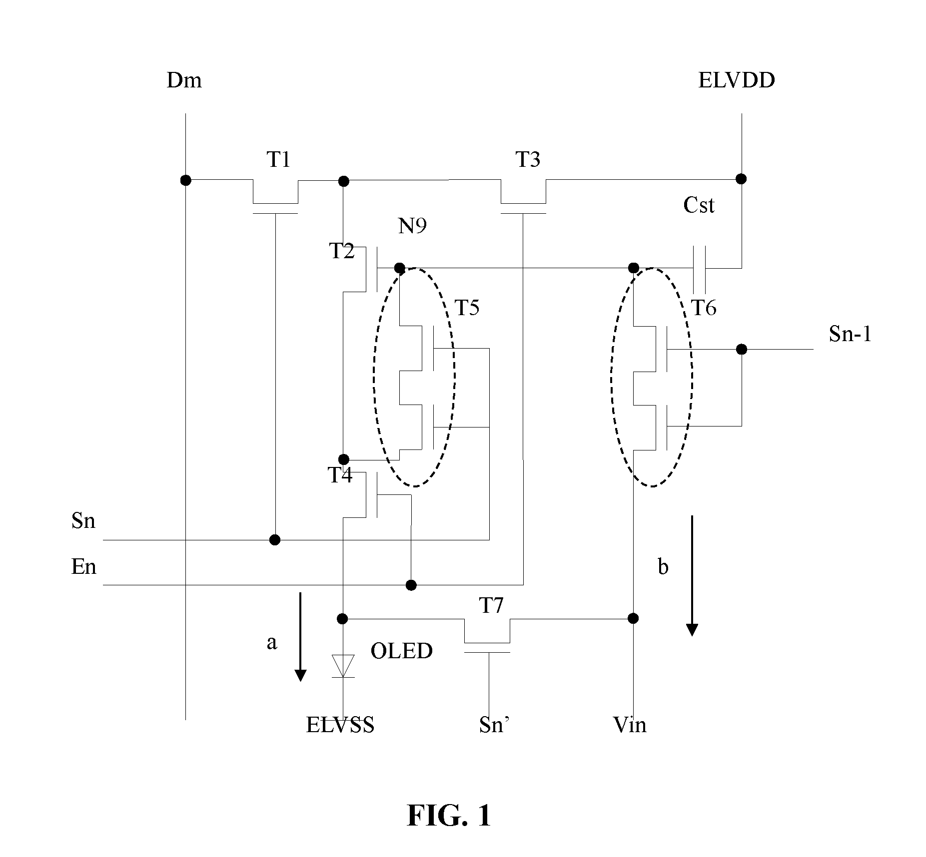
[0110]FIGS. 8 and 9 show two examples of the circuit diagram of the OLED pixel compensation circuit of a second embodiment according to the present invention.

[0111]Specifically, the driving module 10 includes a driving transistor M1. The driving transistor M1 includes a first electrode connected to the second terminal of the first switch module 60. The driving transistor M1 further includes a second electrode connected to the first terminal of the second switch module 70. The driving transistor M1 further includes a gate connected to the second terminal of the compensation module 20, the first terminal of the initialization module 50, and the second terminal of the voltage storage module 90. The first electrode of the driving transistor M1 serves as the first terminal of the driving module 10. The second electrode of the driving transistor M1 serves as the second terminal of the driving module 10. The gate of the driving transistor M1 serves as the control terminal of the driving mo...


PUM


Abstract

An organic light-emitting diode (OLED) pixel compensation circuit includes a driving module, a compensation module, an OLED lighting module, and a precharging module. The compensation module is connected to the driving module and is configured to receive a voltage of an external first power for compensating a turn-on voltage of the driving module. The precharging module is connected to the OLED lighting module and is configured to receive a voltage of an external second power for precharging the OLED lighting module. The driving module is connected to the OLED lighting module and is configured to remain on under compensation by the compensation module for receiving the voltage of the external first power to obtain a driving voltage for driving the OLED lighting module to emit light, thereby driving the OLED lighting module to emit light.

Description

CROSS-REFERENCE TO RELATED INVENTIONS[0001]The present invention claims priority to and the benefit of Chinese Patent invention No. CN ______, filed on ______, the entire content of which is incorporated herein by reference.BACKGROUND OF THE INVENTION[0002]The present invention relates to a circuit and, more particularly, to an organic light-emitting diode (OLED) pixel compensation diode.[0003]Organic light-emitting diodes are essential new element for flat panel display devices and have wide applications due to the advantages of self-illumination, high contrast ratio, wide color gamut as well as simple production technology, low cost, low power consumption, and ease of fulfilling flexible display.[0004]Despite the above advantages, OLED display devices incur many problems during applications. For example, in a thin film transistor (TFT) using an OLED as a switch or a driving element, the stability of the gate voltage is critical, particularly in the black state. If the gate voltage...

Claims


Application Information

Patent Timeline
IPC IPC(8): G09G3/3258G09G3/3291G09G3/3266
CPCG09G3/3258G09G3/3266G09G3/3291G09G2300/0819G09G2320/0238G09G2310/0251G09G2320/045G09G2310/0262G09G2300/0842G09G2300/0814G09G2300/0861G09G2310/08G09G2320/0233G09G2320/043
Inventor ZHOU, XINGYU
Owner EVERDISPLAY OPTRONICS (SHANGHAI) CO LTD
Why Eureka
Try Eureka