
Plasma treatment to improve adhesion between hardmask film and silicon oxide film

a technology of hardmask film and silicon oxide film, which is applied in the manufacture of basic electric elements, semiconductor/solid-state devices, electrical equipment, etc., can solve the problems of undesired particle problems, poor adhesion between the amorphous carbon hardmask layer and the additional mask layer, and low quality patterning

Active Publication Date: 2016-10-27
APPLIED MATERIALS INC
View PDF15 Cites 121 Cited by
  • Summary
  • Abstract
  • Description
  • Claims
  • Application Information

AI Technical Summary

Benefits of technology

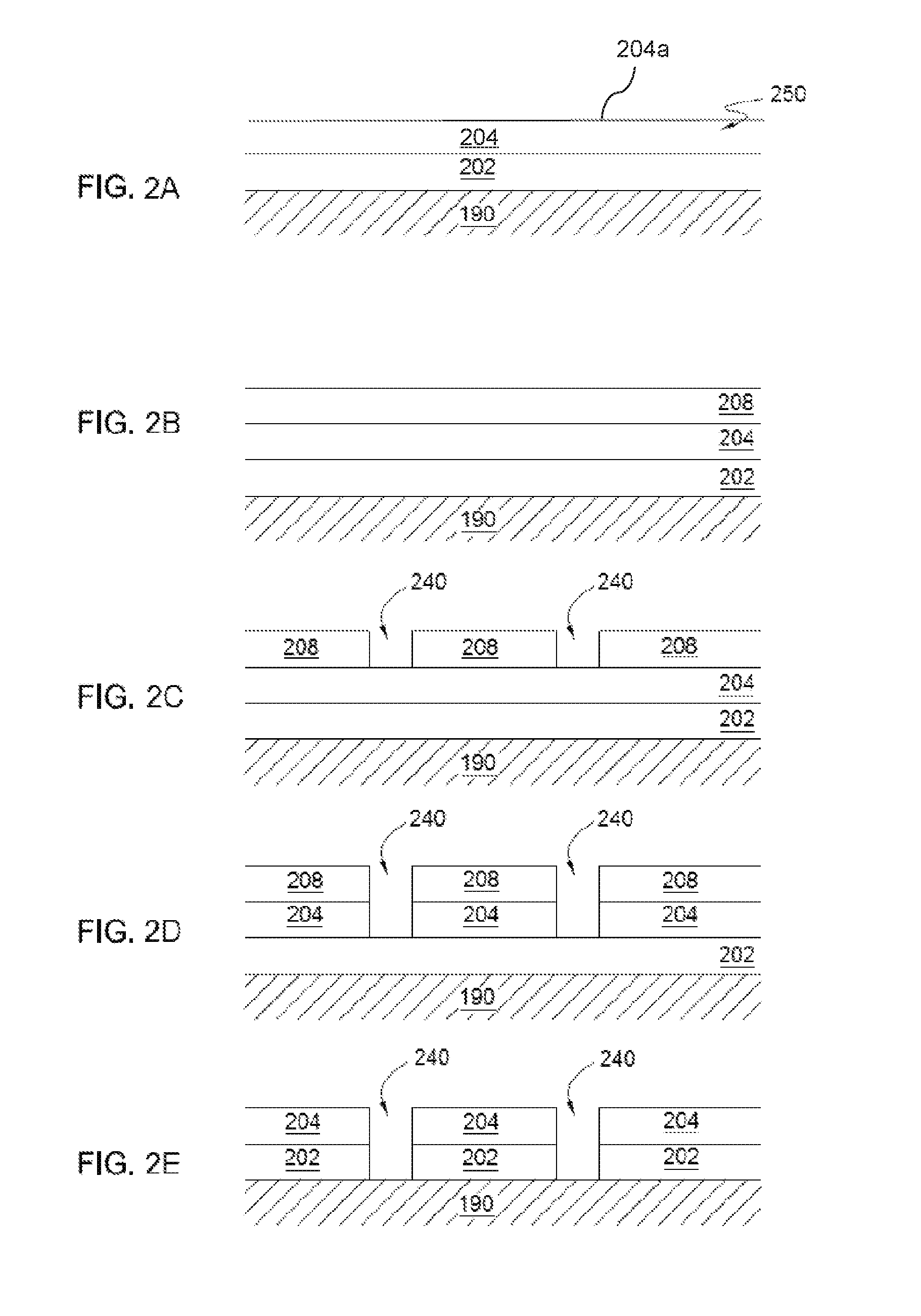
This patent describes methods for making integrated circuits and patterning a hardmask layer. The methods involve depositing a metal-doped amorphous carbon layer onto a substrate and then treating it with plasma. A mask layer is then deposited over the treated layer. The methods allow for precise patterning of the hardmask layer, which is useful in the fabrication of integrated circuits.

Problems solved by technology

However, poor adhesion has been observed between the amorphous carbon hardmask layer and the additional mask layer, such as a silicon oxide layer.
The poor adhesion may result in undesired particle problems or low quality patterning.

Method used


Image

  • Plasma treatment to improve adhesion between hardmask film and silicon oxide film
  • Plasma treatment to improve adhesion between hardmask film and silicon oxide film
  • Plasma treatment to improve adhesion between hardmask film and silicon oxide film

Examples


Embodiment Construction

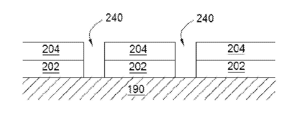
[0017]Embodiments of the present disclosure generally relate to the fabrication of integrated circuits and particularly to patterning a hardmask layer, more particularly, to patterning a metal-doped amorphous carbon layer for use as a hardmask for etching the underlying layer, layer stack, or structure.

[0018]In various embodiments, a plasma treatment may be performed to a synthesis of amorphous carbon films doped with transition metals prior to forming an additional mask layer thereon. The plasma treatment may be performed by exposing the amorphous carbon films to a plasma of argon gas or hydrogen gas. Details of the disclosure and various implementations are discussed below

Exemplary Chamber Hardware for Deposition Process

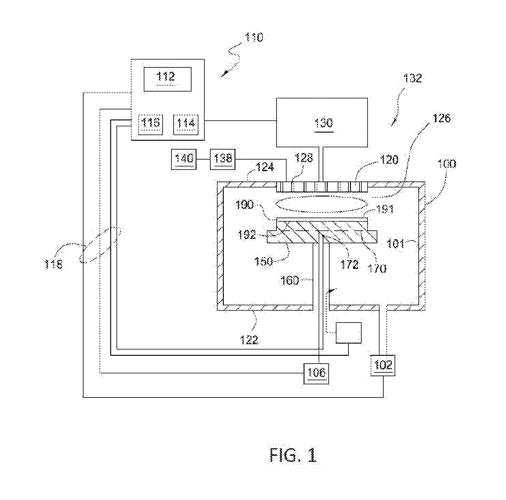
[0019]FIG. 1 is a schematic representation of a substrate processing system 132, which can be used for plasma treatment of an amorphous carbon layer according to embodiments described herein. The substrate processing system 132 may also be used to deposit a doped a...


PUM


Abstract

The present disclosure relates to methods for improving adhesion between a hardmask layer and a subsequent layer on the hardmask layer. Particularly, embodiment of the present disclosure relates to methods for improving adhesion between a metal-doped amorphous carbon layer and a mask layer, such as a silicon oxide layer, a silicon nitride layer, or an amorphous silicon layer. One embodiment of the present disclosure includes performing a plasma treatment to the metal-doped amorphous carbon layer.

Description

CROSS-REFERENCE TO RELATED APPLICATIONS[0001]This application claims priority to U.S. Provisional Patent Application Ser. No. 62 / 151,140, filed on Apr. 22, 2015, which herein is incorporated by reference.BACKGROUND[0002]1. Field[0003]Embodiments of the present disclosure generally relate to the fabrication of integrated circuits and particularly to patterning hardmask materials, such as amorphous carbon.[0004]2. Description of the Related Art[0005]Development of etch selective hardmask materials is an important task for patterning new generation NAND (negative-AND) and DRAM (dynamic random-access memory) devices. Carbon-based materials, such as amorphous carbon (denoted as a-C), has been proved to be an effective material serving as etch hardmask for silicon oxide, silicon nitride, poly-crystalline silicon, or metal (e.g., aluminum) materials due to its chemical inertness, optical transparency, and good mechanical properties. During fabrication, an additional mask layer, such as sil...

Claims


Application Information

Patent Timeline
IPC IPC(8): H01L21/02H01L21/033H01L21/32
CPCH01L21/0234H01L21/02115H01L21/0332H01L21/32H01L21/02274H01L21/3105
Inventor CHENG, RUIMANNA, PRAMITMALLICK, ABHIJIT BASU
Owner APPLIED MATERIALS INC
Learn More