Semiconductor device, memory circuit, method of manufacturing semiconductor device

a memory circuit and semiconductor technology, applied in the direction of semiconductor devices, electrical appliances, basic electric elements, etc., can solve the problems of major leakage current and increase in leakage current, and achieve the effect of improving transistor characteristics, improving transistor characteristics, and increasing channel length and channel width

Active Publication Date: 2016-11-03
SONY CORP
View PDF4 Cites 7 Cited by
  • Summary
  • Abstract
  • Description
  • Claims
  • Application Information

AI Technical Summary

Benefits of technology

[0110]In the following, description is given of effects of the semiconductor device 1 according to the embodiment.
[0111]In the embodiment, the buried gate vertical transistor is provided in the semiconductor layer 10. In the buried gate vertical transistor, the source-drain section 22, the channel section 23, and the source-drain sections 21 are disposed along the normal direction to the semiconductor layer 10, and the gate section 24 is buried in the groove 10A. Accordingly, as compared with a transistor in which all electrodes are provided on top surface side of a semiconductor layer, a channel length and a channel width are easily increased, which makes it possible to improve the transistor characteristics. Moreover, the stress application section is provided. The stress application section applies one of compressive stress and tensile stress to the channel section 23 in the normal direction to the semiconductor layer 10. This makes it possible to further improve the transistor characteristics. Further, the electrode section 25 electrically coupled to the source-drain section 21, and the electrode section 27 electrically coupled to the gate section 24 are provided on the top surface side of the semiconductor layer 10, and the electrode section 26 electrically coupled to the source-drain section 22 is provided on the rear surface side of the semiconductor layer 10. This makes it possible to reduce occupancy area, as compared with the transistor in which all electrodes are provided on the top surface side of the semiconductor layer. Accordingly, it is possible to cope with design shrinkage while improving the transistor characteristics.
[0112]In the following, description is given of modification examples of the semiconductor device 1 according to the foregoing embodiment. It is to be noted that same component as the components of the semiconductor device 1 according to the foregoing embodiment are denoted by same reference numerals. Further, description of the same components as the components of the semiconductor device 1 according to the foregoing embodiment are omitted as appropriate.

Problems solved by technology

For example, degradation of the short-channel characteristics may cause an increase in a leakage current due to subthreshold leakage during standby.
The leakage current is a major issue specifically in SRAMs and other memories.

Method used


Image

  • Semiconductor device, memory circuit, method of manufacturing semiconductor device
  • Semiconductor device, memory circuit, method of manufacturing semiconductor device
  • Semiconductor device, memory circuit, method of manufacturing semiconductor device

Examples


first embodiment (

1. First Embodiment (Semiconductor Device)

2. Modification Examples of First Embodiment (Semiconductor Device)

second embodiment (

3. Second Embodiment (Memory Circuit)

4. Modification Examples of Second Embodiment (Memory Circuit)

first embodiment

1. First Embodiment

Configuration

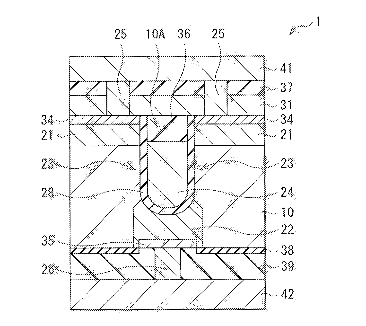
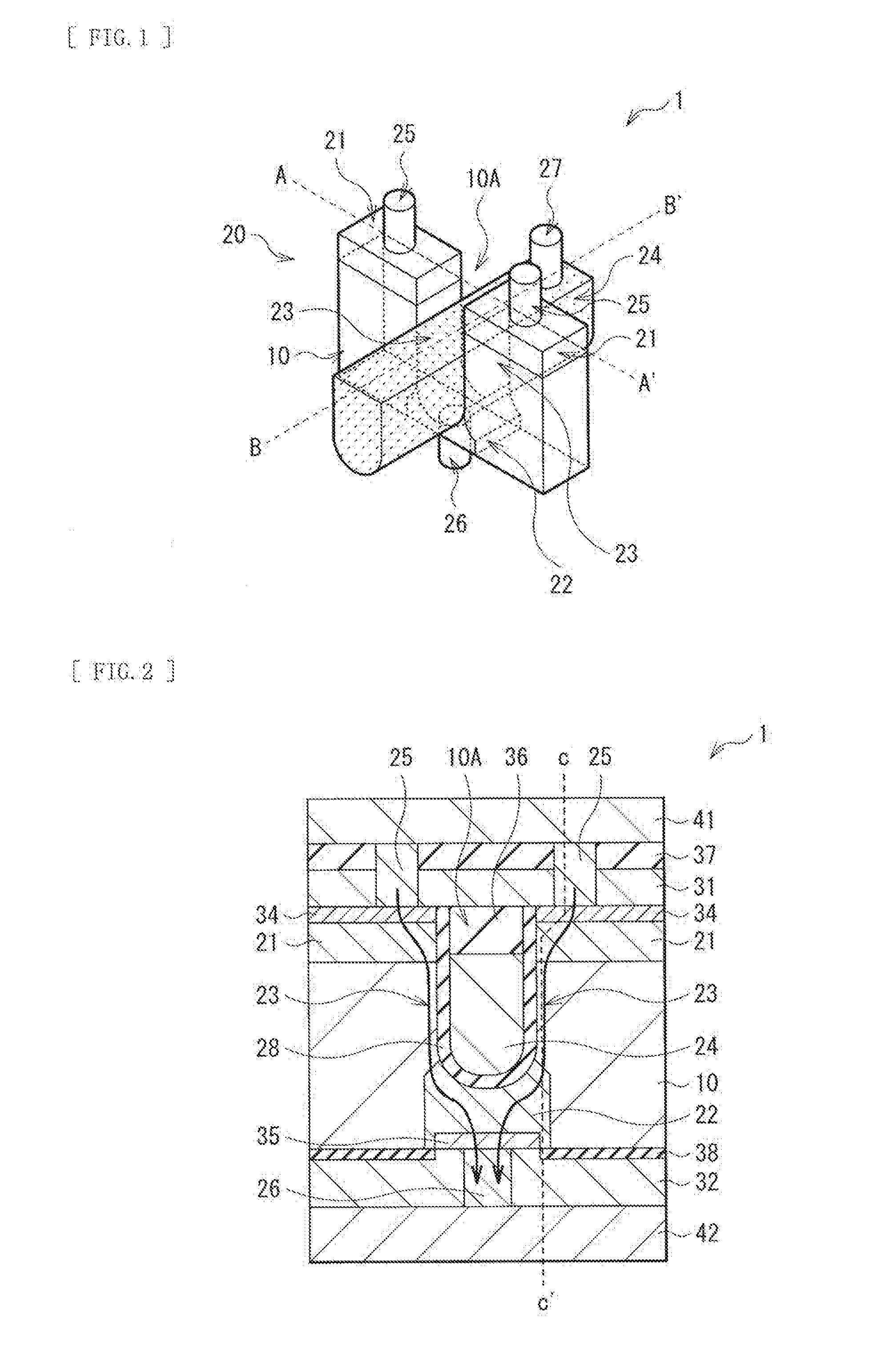
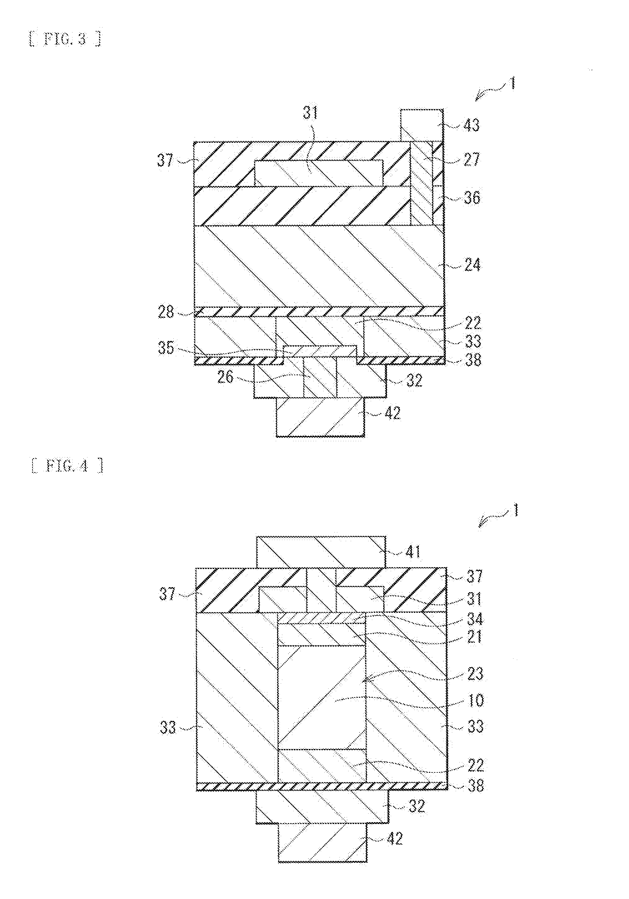
[0085]FIG. 1 illustrates a perspective configuration of a semiconductor device 1 according to a first embodiment of the technology. FIG. 2 illustrates an example of a cross-sectional configuration taken along a line A-A′ of FIG. 1 of the semiconductor device 1. FIG. 3 illustrates an example of a cross-sectional configuration taken along a line B-B′ of FIG. 1 of the semiconductor device 1. FIG. 4 illustrates an example of a cross-sectional configuration taken along a line C-C′ of FIG. 2 of the semiconductor device 1. The semiconductor device 1 includes a semiconductor layer 10 and a transistor 20 that is formed in the semiconductor layer 10.

(Transistor 20)

[0086]The transistor 20 is a buried gate vertical transistor. The transistor 20 may be a p-type MOS transistor or an n-type MOS transistor. The transistor 20 includes two source-drain sections 21, a source-drain section 22, a channel section 23, a gate section 24, an electrode section 25, an electrode...


PUM


Abstract

A semiconductor device of the technology includes a first diffusion section (22), a second diffusion section (21), a channel section (23), a gate section (24), and a stress application section (31, 32, or 33). In a semiconductor layer (10) having a groove (10A), the first diffusion section (22) is formed at or in the vicinity of a bottom of the groove (10A), the second diffusion section (21) is formed at an upper end of the groove (10A), and the channel section (23) is formed between the first diffusion section (22) and the second diffusion section (21). The gate section (24) is buried in the groove (10A) at a position opposing the channel section (23). The stress application section (31, 32, or 33) applies one of compressive stress and tensile stress to the channel section (23) in a normal direction to the semiconductor layer (10).

Description

TECHNICAL FIELD[0001]The technology relates to a semiconductor device in which a channel of a transistor is formed in a normal direction to a substrate surface and a memory circuit including the semiconductor device. Further, the technology relates to a method of manufacturing the semiconductor device.BACKGROUND ART[0002]In the past, performance of LSIs has been improved with advance of technology nodes by design shrinkage in accordance with a scaling law along with Moore's Law. Although 20-nm nodes and 14-nm nodes are currently under development, it is imperative to suppress short-channel characteristics of transistors. For example, degradation of the short-channel characteristics may cause an increase in a leakage current due to subthreshold leakage during standby. The leakage current is a major issue specifically in SRAMs and other memories. In recent years, an urgent task is therefore to reduce power consumption by replacement of volatile memories with non-volatile memories, and...

Claims


Application Information

Patent Timeline
Patent Type & Authority Applications(United States)
IPC IPC(8): H01L27/22H01L29/04H01L29/768H01L43/02H01L21/8234H01L29/423
CPCH01L27/228H01L21/823406H01L21/823487H01L29/045H01L29/768H01L43/02H01L29/42396H01L29/7827H01L29/7843H01L29/7846H01L29/66666H10B63/34H10B61/22H10N50/80
Inventor YOKOYAMA, TAKASHIUMEBAYASHI, TAKU
Owner SONY CORP
Why Eureka
Try Eureka