

Compound semiconductor device and manufacturing method thereof
A manufacturing method and semiconductor technology, applied in semiconductor/solid-state device manufacturing, semiconductor devices, amplifiers, etc., can solve problems such as device threshold changes
- Summary
- Abstract
- Description
- Claims
- Application Information
AI Technical Summary
Problems solved by technology
Method used
Image

Examples
no. 1 example
[0021] In this embodiment, an MIS-type AlGaN / GaN HEMT is disclosed as a compound semiconductor device.
[0022] Figure 1A to Figure 3C is a schematic cross-sectional view showing a method of manufacturing the MIS-type AlGaN / GaN HEMT according to the first embodiment in process order. For the sake of illustration, in Figure 2A to Figure 3A In , only the vicinity of the gate is shown in an enlarged manner.
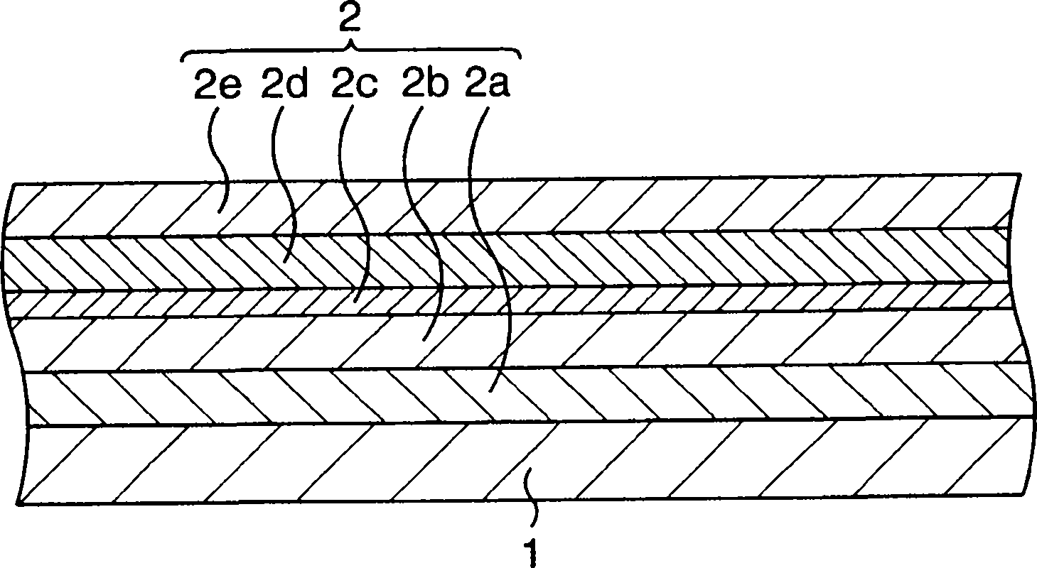
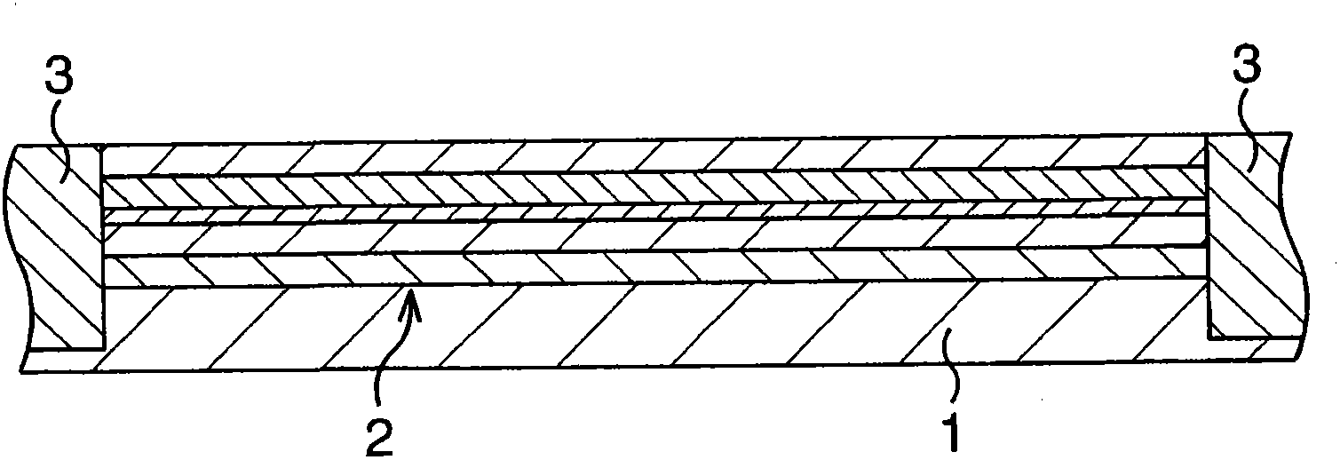
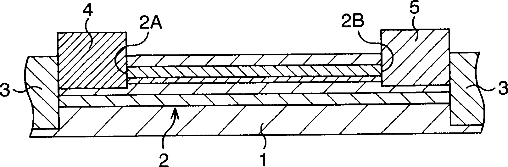
[0023] First, if Figure 1A As shown, for example, a compound semiconductor layer 2 is formed on a semi-insulating silicon carbide substrate 1 as a growth substrate. The compound semiconductor layer 2 includes a buffer layer 2a, an electron transit layer 2b, an intermediate layer 2c, an electron supply layer 2d, and a capping layer 2e. In the AlGaN / GaN HEMT, a two-dimensional electron gas (2DEG) is generated in the vicinity of the interface of the electron transit layer 2b and the electron supply layer 2d (more precisely, the intermediate layer 2c).
[0024] More spec...
no. 2 example
[0072] In this embodiment, a Schottky-type AlGaN / GaN HEMT is disclosed as a compound semiconductor device.
[0073] Image 6 It is a schematic cross-sectional view showing main processes of the method of manufacturing the Schottky-type AlGaN / GaN HEMT according to the second embodiment.
[0074] First, as in the first embodiment, execute Figure 1A to Figure 3A process to apply a fluorine termination treatment on the surface of the compound semiconductor layer 2 .
[0075] Subsequently, if Image 6 As shown, a gate 7 is formed.
[0076] More specifically, first, a lower resist (for example, product name PMGI: manufactured by U.S. MicroChem Corporation) and an upper resist (for example, product name PFI32-A8) are applied and formed on the compound semiconductor layer 2 by, for example, a spin coating method. : manufactured by Sumitomo Chemical Co., Ltd.). Openings, eg, about 0.8 μm in diameter, are formed in the upper resist by ultraviolet exposure. Next, using the upper r...
no. 3 example
[0080] In this embodiment, a power supply device including an AlGaN / GaN HEMT selected from the first embodiment and the second embodiment is disclosed.
[0081] Figure 7 is a connection diagram showing a schematic structure of a power supply device according to the third embodiment.
[0082] The power supply device according to this embodiment includes: a high-voltage primary circuit 21 , a low-voltage secondary circuit 22 ; and a transistor 23 disposed between the primary circuit 21 and the secondary circuit 22 .
[0083] The primary circuit 21 includes an AC power source 24, a so-called bridge rectifier circuit 25, and a plurality of (here, four) switching elements 26a, 26b, 26c, and 26d. Further, the bridge rectifier circuit 25 has a switching element 26e.
[0084] The secondary circuit 22 includes a plurality of (here, three) switching elements 27a, 27b, and 27c.
[0085] In this embodiment, each of the switching elements 26a, 26b, 26c, 26d, 26e of the primary circuit ...
PUM
 Abstract
Description
Claims
Application Information