Transistor and manufacturing method of transistor

a manufacturing method and transistor technology, applied in the direction of transistors, semiconductor devices, electrical apparatus, etc., can solve the problems of poor product quality, difficult microfabrication, and inability to achieve high alignment accuracy, and achieve high electrical connection reliability, good transistor characteristics, and high productivity

Inactive Publication Date: 2019-04-02
FUJIFILM CORP
View PDF11 Cites 0 Cited by
  • Summary
  • Abstract
  • Description
  • Claims
  • Application Information

AI Technical Summary

Benefits of technology

[0018]The present invention has been made for solving such problems of the technology of the related art, and an object of the present invention is to provide an air gap type transistor which has high electrical connection reliability and high productivity and is capable of exhibiting good transistor characteristics while achieving microfabrication, and a manufacturing method of a transistor.
[0046]According to the present invention, it is possible for an air gap type transistor to achieve high electrical connection reliability and high productivity and to exhibit good transistor characteristics while achieving microfabrication.

Problems solved by technology

However, in a case of laminating the organic semiconductor crystal that is separately formed on the electrodes, there is a problem that high alignment accuracy cannot be achieved and microfabrication is difficult or productivity is deteriorated.
In addition, the configuration in which the organic semiconductor crystal is laminated on the source electrode and the drain electrode using the source electrode and the drain electrode as supports is merely for physically adsorbing the organic semiconductor crystal, and thus, there are problems of low electrical connection reliability and low transistor characteristics.

Method used


Image

  • Transistor and manufacturing method of transistor
  • Transistor and manufacturing method of transistor
  • Transistor and manufacturing method of transistor

Examples


example 1

[0174]

[0175](Preparation Step)

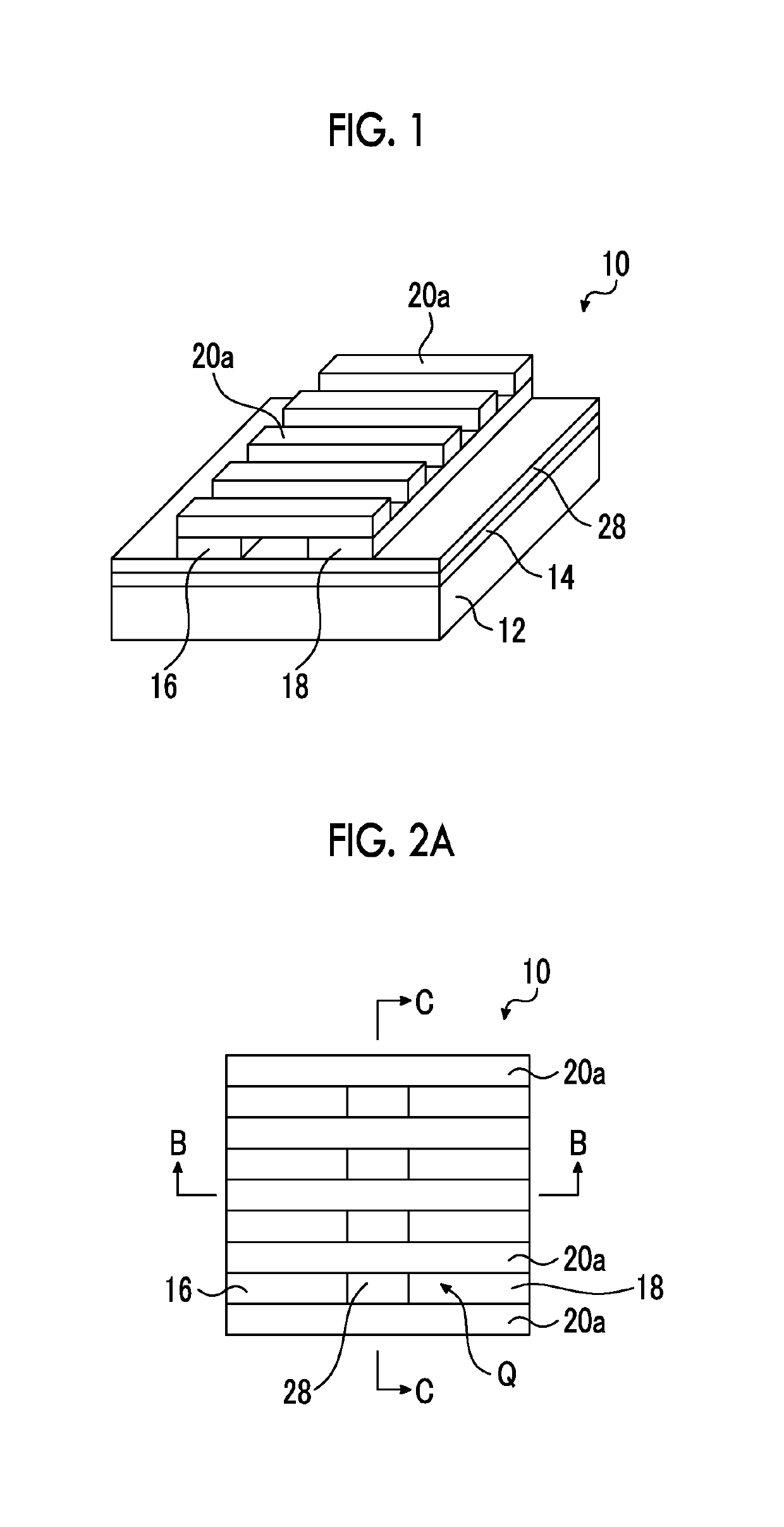
[0176]Alkali-free glass having a thickness of 0.7 mm and a size of 50 mm×50 mm (EAGLE XG, manufactured by Corning Incorporated) was used as the substrate 12.

[0177]Chrome (Cr: 0.01 μm thickness) and silver (Ag: 0.04 μm thickness) were sequentially vacuum-vapor deposited on the alkali-free glass substrate 12 by using a general vacuum vapor deposition apparatus to form the gate electrode layer 14.

[0178]Next, an aluminum oxide (AlOx: 0.2 μm thickness) film was formed on the Gate electrode layer 14 as the solid insulating layer 28 by high frequency magnetron sputtering using a general high frequency magnetron sputtering apparatus.

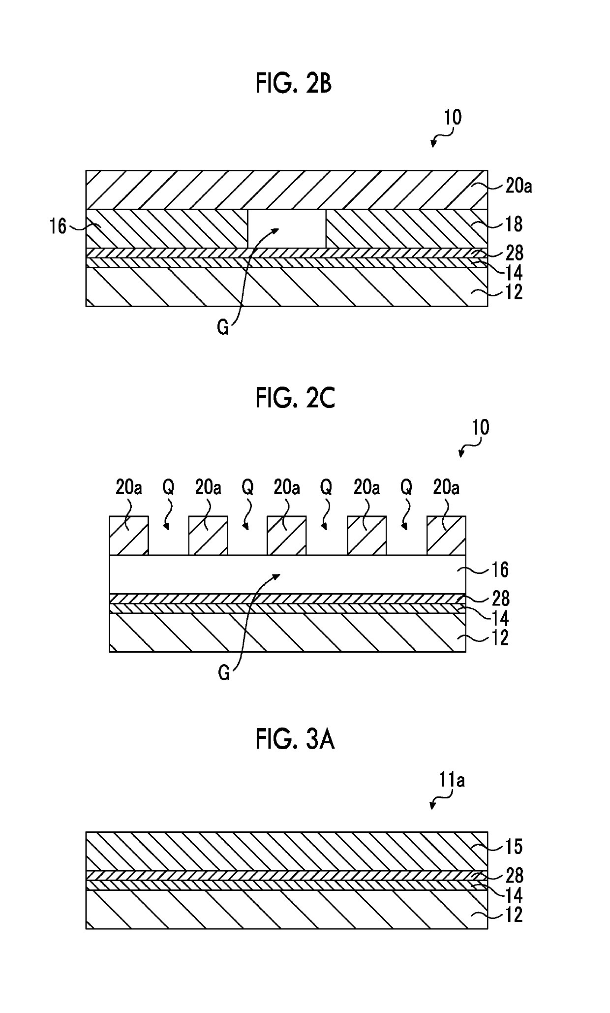
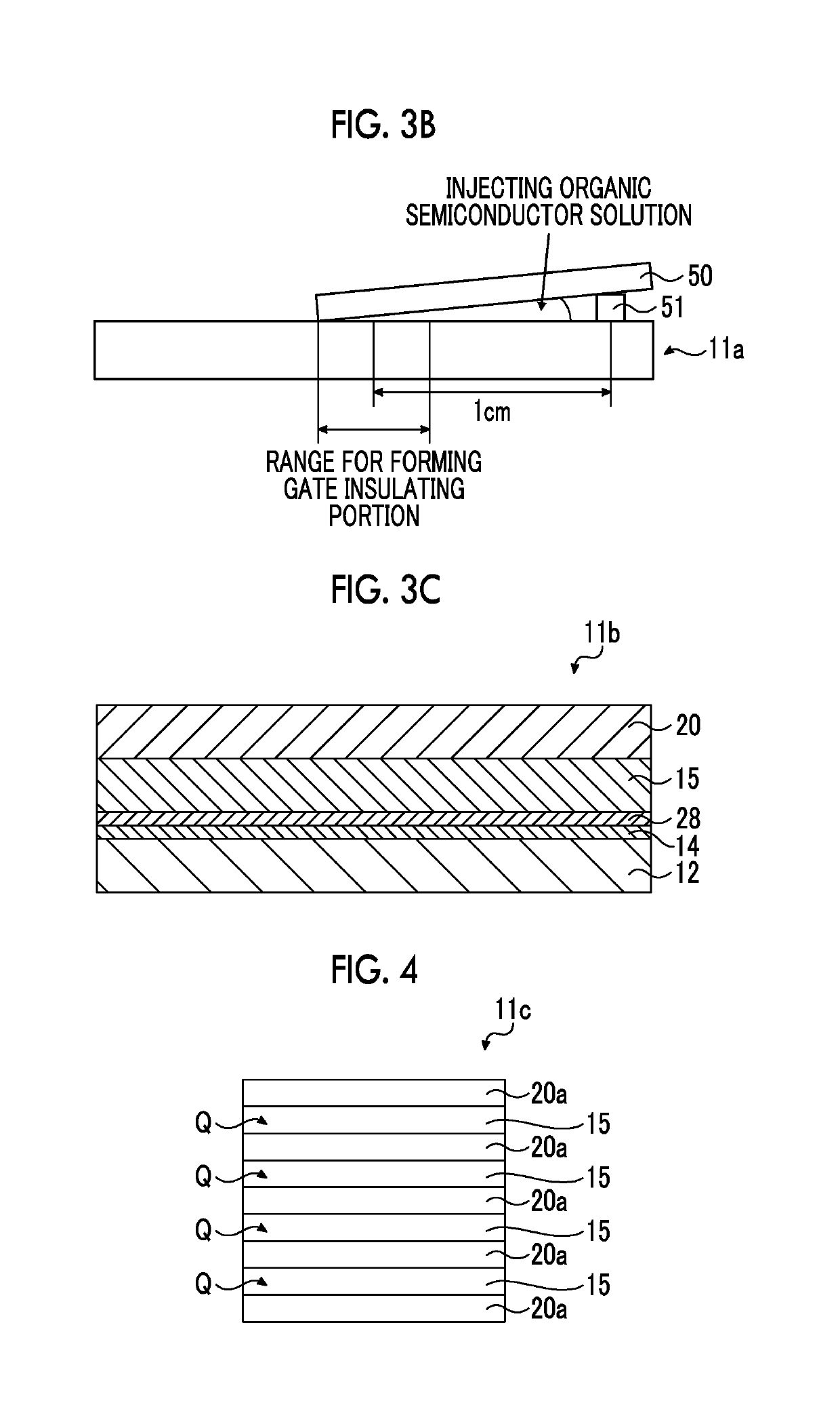
[0179]Further, a gold film (Au: 1 μm thickness) was formed on the solid insulating layer 28 as the support precursor layer 15 by using a general sputtering apparatus to prepare the laminate 11a.

[0180](Semiconductor Layer Forming Step)

[0181]A semiconductor layer (1 μm thickness) was formed on the support precursor layer 15 of the pr...

example 2

[0195]A transistor was prepared in the same manner as in Example 1 except that the etching step in the support forming step was changed.

[0196]Specifically, the laminate 11d was immersed in the Au etching solution (AURUM-304, manufactured by KANTO CHEMICAL CO., INC.) for 5 minutes. Next, the laminate was immersed in an aqueous solution of tetramethyl ammonium hydroxide (TMAH: 2.38%) for 2 hours and then washed by being immersed in pure water for half a day. The laminate was further immersed in a hydrofluoroether-alcohol mixed solvent (Novec 71IPA, manufactured by 3M Japan Limited) for 10 minutes and then was dried naturally. Furthermore, vacuum drying was performed for a day.

[0197]As a result, the support precursor layer 15 and the solid insulating layer 28 corresponding to the region between the two etching protective layers 30a and 30b were removed and thus the transistor 40 as shown in FIG. 7 was prepared. That is, the insulating layer removing step was provided.

example 3

[0198]A transistor was prepared in the same manner as in Example 1 except that in the opening portion forming step, the shape of the opening portion Q to be formed was changed to a shape shown in FIG. 8. In this case, the formation pattern of the opening portions Q is set to Pattern B.

[0199]The number of opening portions Q was set to 10 and the size of the opening portion was set to 20 μm×100 μm. In addition, the outer peripheral portion of the semiconductor layer 20f was also removed by irradiation with a laser and the size of the entire semiconductor layer 20f was set to a width of 1 mm×a depth of 0.4 mm.


PUM


Abstract

Provided are an air up type transistor which has high electrical connection reliability and high productivity, and is capable of exhibiting good transistor characteristics while achieving microfabrication, and a manufacturing method of a transistor. A semiconductor layer is formed on an upper surface of a support precursor layer which becomes a semiconductor layer support and then a part of the semiconductor layer is removed to form one or more opening portions from which the support precursor layer is exposed. Two etching protective layers are formed on the semiconductor layer such that the two etching protective layers are separated from each other and at least a part of the opening portion is positioned in a region between the two etching protective layers. A part of the support precursor layer is removed by bringing an etchant into contact with the support precursor layer through the plurality of opening portions, thereby forming a space at a position corresponding to a region between the two etching protective layers so as to form two semiconductor layer supports that are arranged with the space interposed therebetween.

Description

CROSS-REFERENCE TO RELATED APPLICATIONS[0001]This application is a Continuation of PCT International Application No. PCT / JP2016 / 059572 filed on Mar. 25, 2016, which claims priority under 35 U.S.C. § 119(a) to Japanese Patent Application No. 2015-063065 filed on Mar. 25, 2015. The above application is hereby expressly incorporated by reference, in its entirety, into the present application.BACKGROUND OF THE INVENTION1. Field of the Invention[0002]The present invention relates to a transistor and a manufacturing method of a transistor.2. Description of the Related Art[0003]A thin film transistor (TFT) has been used in a display, a solid image pickup element, a transistor circuit, a radio frequency identifier (RFID), and the like. In particular, it is expected that a TFT using a coating type semiconductor can prepare a large-area TFT at a low cost by using a printing step together.[0004]A structure of a TFT includes various forms according to an arrangement position of a gate electrode...

Claims


Application Information

Patent Timeline
Patent Type & Authority Patents(United States)
IPC IPC(8): H01L29/66H01L51/05H01L29/786H01L29/423H01L21/311
CPCH01L29/66742H01L21/31105H01L51/0558H01L29/78696H01L29/42356H10K10/484
Inventor MAEHARA, YOSHIKI
Owner FUJIFILM CORP
Why Eureka
Try Eureka