Semiconductor device with copper wirings

a technology of semiconductor devices and wirings, applied in semiconductor devices, semiconductor/solid-state device details, radiation controlled devices, etc., can solve the problems of nbti deterioration and increase of nbti deterioration, and achieve the effect of suppressing nbti deterioration

Inactive Publication Date: 2005-02-10
SOCIONEXT INC
View PDF9 Cites 3 Cited by
  • Summary
  • Abstract
  • Description
  • Claims
  • Application Information

AI Technical Summary

Benefits of technology

[0015] An object of this invention is to provide a semiconductor devi...

Problems solved by technology

Even if a gate insulating film is made thick to lower direct tunneling current, the NBTI deterioration poses a problem.
If the nitrogen concentration in a gate insulat...

Method used


Image

  • Semiconductor device with copper wirings
  • Semiconductor device with copper wirings
  • Semiconductor device with copper wirings

Examples


Embodiment Construction

[0031] First, the experiments made by the present inventors and their results will be described.

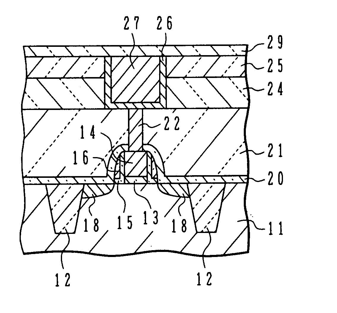
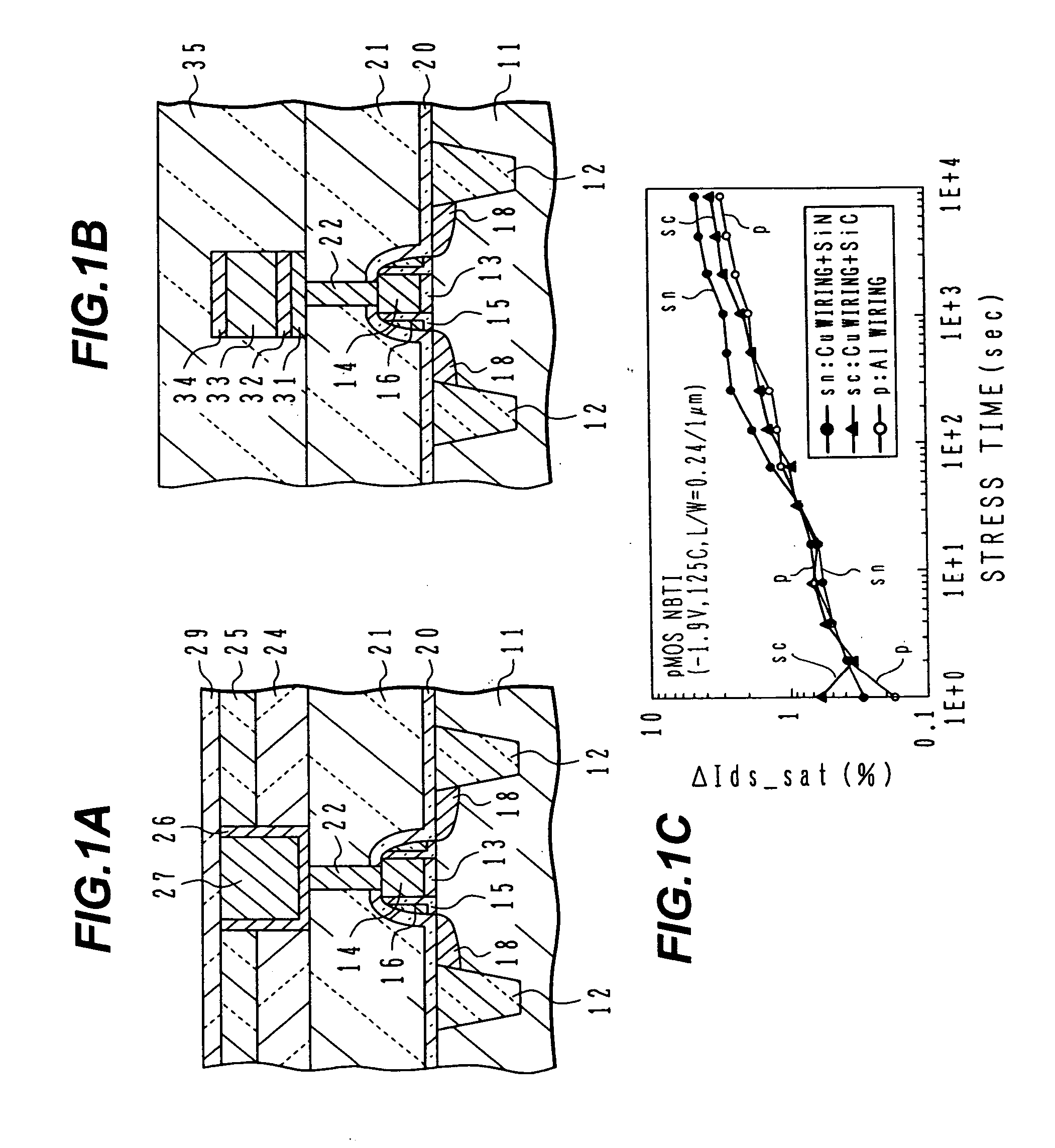
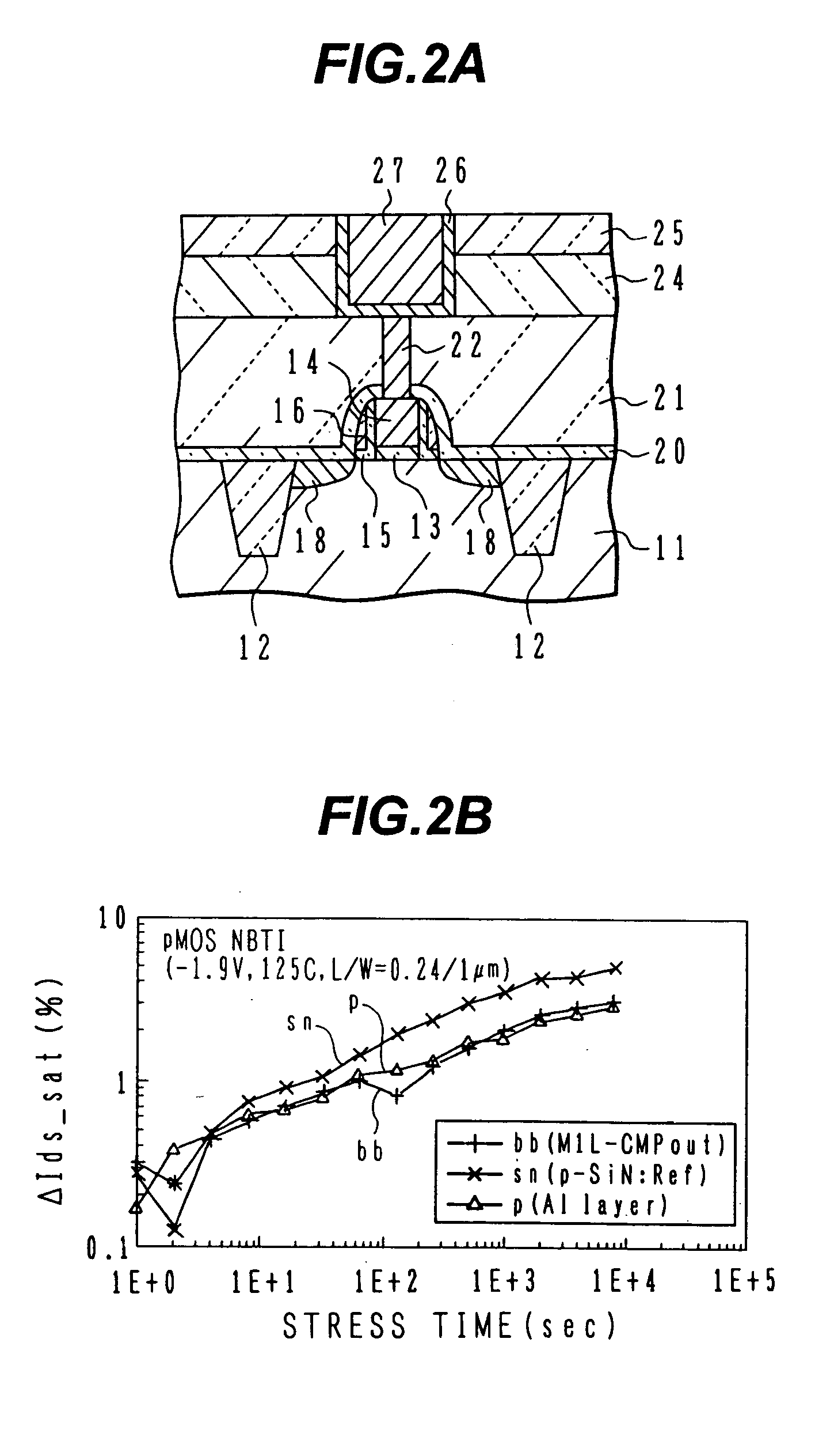
[0032]FIG. 1A is a cross sectional view showing the structure of a sample used for preliminary experiments. An etching mask of photoresist is formed on the surface of a silicon substrate 11, and the silicon substrate 11 is etched, for example, to a depth of 300 nm to form a trench. Burying the trench, a silicon oxide film is deposited to a thickness of, e.g., about 500 nm. The silicon oxide film on the surface of the silicon substrate 11 is removed by chemical mechanical polishing (CMP). A silicon oxide film 12 is left only in the trench to form shallow trench isolation (STI).

[0033] A resist pattern is formed having an opening corresponding to a well region, and P+ ions are implanted into the silicon substrate 11 at an acceleration energy of 600 keV and at a dose of 3×1013 cm−2 to form an n-well.

[0034] A gate insulating film 13 of silicon oxide which contains 4 at % nitrogen is formed ...


PUM


Abstract

A semiconductor device with p-channel MOS transistor having: a gate insulating film of nitrogen-containing silicon oxide; a gate electrode of boron-containing silicon; side wall spacers on side walls of the gate electrode, comprising silicon oxide; an interlayer insulating film having a planarized surface; a wiring trench and a contact via hole formed in the interlayer insulating film; a copper wiring pattern including an underlying barrier layer and an upper level copper region, and filled in the wiring trench; and a silicon carbide layer covering the copper wiring pattern. A semiconductor device has the transistor structure capable of suppressing NBTI deterioration.

Description

CROSS REFERENCE TO RELATED APPLICATION [0001] This application is based on Japanese Patent Application No. 2002-091306, filed on Mar. 28, 2002, the entire contents of which are incorporated herein by reference. BACKGROUND OF THE INVENTION [0002] A) Field of the Invention [0003] The present invention relates to a semiconductor device, and more particularly to a semiconductor device with copper wirings. [0004] B) Description of the Related Art [0005] In order to realize high speed operation and low power consumption of LSI circuits, device elements are made fine, and drive voltage and resistance of wiring are reduced. In order to lower the resistance of wiring, Cu wiring having a lower resistivity than conventionally used Al wiring is adopted. Fine patterning of a Cu layer is difficult so that a damascene structure is often adopted. For fine device elements and low power consumption, it is desired to realize a high speed operation of transistor at a low voltage. To this end, a gate in...

Claims


Application Information

Patent Timeline
IPC IPC(8): H01L21/28H01L21/768H01L21/8234H01L23/532H01L27/088H01L29/78
CPCH01L21/28202H01L21/76807H01L21/76828H01L21/76834H01L21/76843H01L21/76846H01L2924/0002H01L23/53238H01L29/518H01L2924/00H01L21/823871H01L21/3205
Inventor KAKAMU, KATSUMITAKAO, YOSHIHIRO
Owner SOCIONEXT INC
Why Eureka
Try Eureka