Electrochemically-gated field-effect transistor, methods for its manufacture and use thereof

Inactive Publication Date: 2015-01-06
KARLSRUHER INST FUR TECH
View PDF8 Cites 2 Cited by
  • Summary
  • Abstract
  • Description
  • Claims
  • Application Information

AI Technical Summary

Benefits of technology

[0075]Therefore, high-performance single- or multi-nanowire devices are easily obtained by using a solution-processed and/or printed polymer-based electrolyte, where the operating voltages do not exceed 5 V, preferabl

Problems solved by technology

Generally, a combination of a Si/SiO2 gate/gate oxide is used which classifies these devices as power transistors since a high-voltage source is required for their operation which, at the same time, limits their field of applications.
However, these self-assembled, high-k organic dielectrics are difficult to scale up to be used in electronic devices which

Method used


Image

  • Electrochemically-gated field-effect transistor, methods for its manufacture and use thereof
  • Electrochemically-gated field-effect transistor, methods for its manufacture and use thereof
  • Electrochemically-gated field-effect transistor, methods for its manufacture and use thereof

Examples


Example

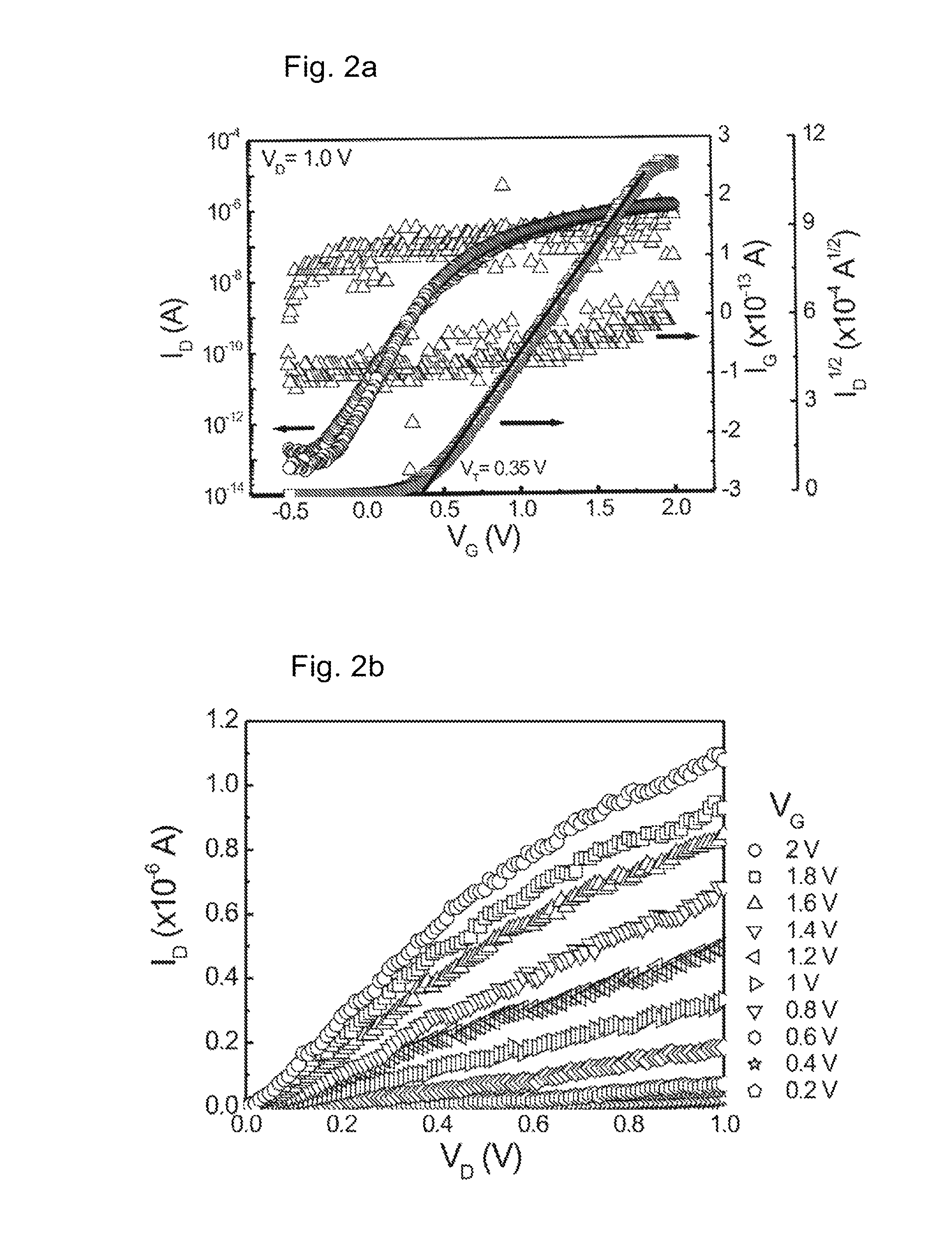
[0080]Nanowires were prepared with a vapour liquid solid mechanism (VLS). The nanowires were placed on the substrates of the device by simply tapping the donor substrate on a receiver substrate (device substrate). Conventional e-beam lithography was used to build the devices. Using RF sputtering, tin doped indium oxide (ITO) has been deposited as electrodes on the nanowire. FET devices were made either with ZnO or SnO2 nanowires, ITO electrodes were used as passive structures and an ink-jet printed highly transparent composite solid polymer-based electrolyte was used as a surround gate dielectric for the fabricated single nanowire channel transistor device.

[0081]An electrolyte was employed which consisted of the synthetic polymer poly(vinyl alcohol), PVA, the plasticizer propylene carbonate, PC, the supporting electrolyte (salt) LiClO4, and the solvent dimethyl sulfoxide, DMSO.

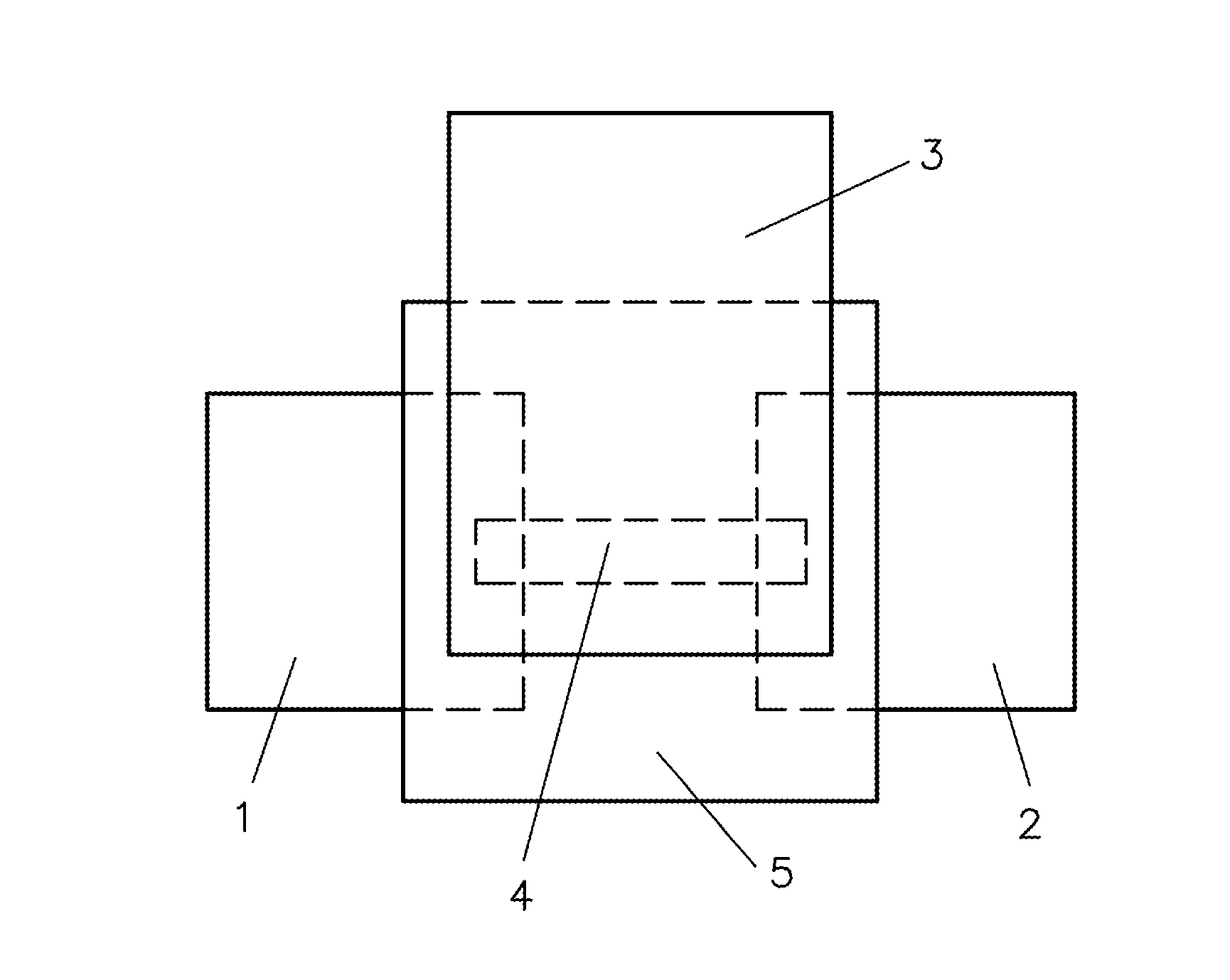
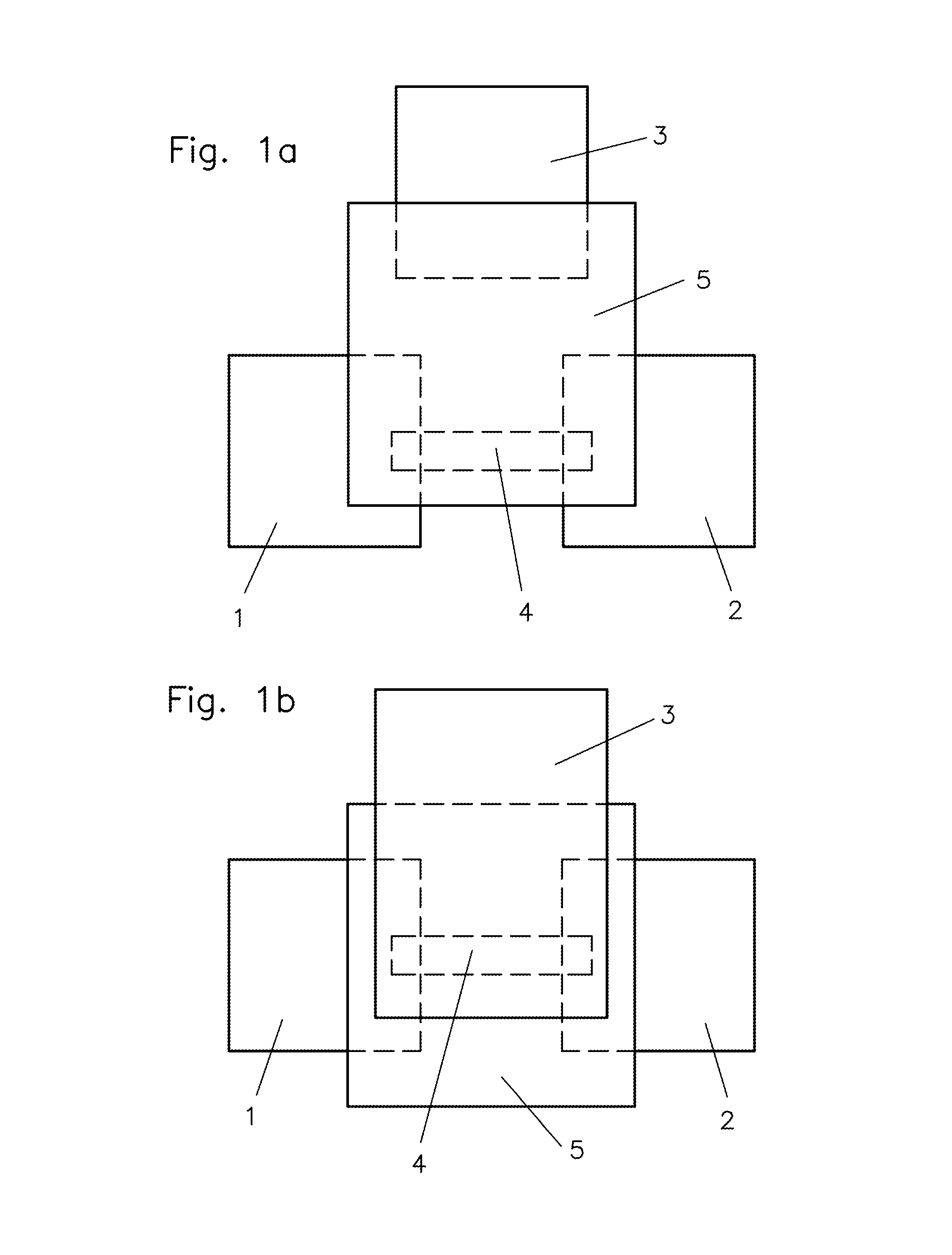
[0082]FIG. 1 shows two different schemes of single-nanowire FETs. Whereas FIG. 1a) depicts an in-plane FET,...


PUM


Abstract

An electrochemically-gated field-effect transistor includes a source electrode, a drain electrode, a gate electrode, a transistor channel and an electrolyte. The transistor channel is located between the source electrode and the drain electrode. The electrolyte completely covers the transistor channel and has a one-dimensional nanostructure and a solid polymer-based electrolyte that is employed as the electrolyte.

Description

BACKGROUND OF THE INVENTION[0001]1. Field of the Invention[0002]For the purpose of explaining the development of one-dimensional nanostructure electronics, the following citations will be referenced:[0003]The present invention relates to an electrochemically-gated field-effect transistor (FET), to methods for its manufacture, to its use, and to electronics comprising said field-effect transistor.[0004]2. Description of the Prior Art[0005][1] Kim et al., “Fabrication of reliable semiconductor nanowires by controlling crystalline structure,” Nanotechnology 22 (2011), 305704, 6 pages.[0006][2] Taekyung Lim, et al., “A nanowire-based shift register for display scan drivers,” Nanotechnology 22 (2011), 405203, 7 pages.[0007][3] Park et al., “Effect of gate dielectrics on the device performance of SnO2 nanowire field effect transistors,” Applied Physics Letters, 96, 102908 (2010), 4 pages.[0008][4] Ju et al., “High performance ZnO nanowire field effect transistors with organic gate nanodie...

Claims


Application Information

Patent Timeline
IPC IPC(8): H01L29/06H01L29/08G01N27/414H01L51/05
CPCH01L51/0562G01N27/4146H01L51/0558H01L29/0665H01L29/0669B82Y10/00H10K10/486H10K10/484
Inventor DASGUPTA, SUBHOHAHN, HORSTNASR, BABAK
Owner KARLSRUHER INST FUR TECH
Why Eureka
Try Eureka