Manufacturing method of organic semiconductor device

a manufacturing method and semiconductor technology, applied in the direction of semiconductor devices, basic electric elements, electrical appliances, etc., can solve the problems of lowering the performance of the organic transistor to be manufactured, difficult method to manufacture an organic semiconductor device, difficult to transfer an organic semiconductor layer in highly-precise pattern, etc., to achieve excellent transistor characteristics, high production efficiency, and high precision

Inactive Publication Date: 2012-06-19
DAI NIPPON PRINTING CO LTD
View PDF5 Cites 0 Cited by
  • Summary
  • Abstract
  • Description
  • Claims
  • Application Information

AI Technical Summary

Benefits of technology

[0026]The manufacturing method of an organic semiconductor device of the present invention attains the effect of enabling the manufacturing of a highly-productive organic semiconductor device having excellent transistor characteristics by transferring the organic semiconductor layer in highly-precise pattern.

Problems solved by technology

However, the method of Patent Literature 1 has a problem that it is very difficult for the method to manufacture an organic semiconductor device which has such technical structure because it is difficult to form plural organic semiconductor layers in pattern.
However, it is still difficult to transfer an organic semiconductor layers in highly-precise pattern in such method.
Further, to begin with, when an organic transistor is manufactured by such a method, there is a problem of lowering a performance of the organic transistor to be manufactured because alignment of the liquid crystalline organic semiconductor material in the organic semiconductor layer is deteriorated due to the heating of or pressing to the organic semiconductor layer at the time of transferring the organic semiconductor layer.
Although possibility of avoiding such problem remains by transferring the organic semiconductor layer under milder conditions, such conditions will largely limit the transferring conditions, and thereby resulting in raising another problem of making it impossible to manufacture an organic transistor with high productivity.

Method used


Image

  • Manufacturing method of organic semiconductor device
  • Manufacturing method of organic semiconductor device
  • Manufacturing method of organic semiconductor device

Examples


first embodiment

A. First Embodiment for Manufacturing Method of Organic Semiconductor Device

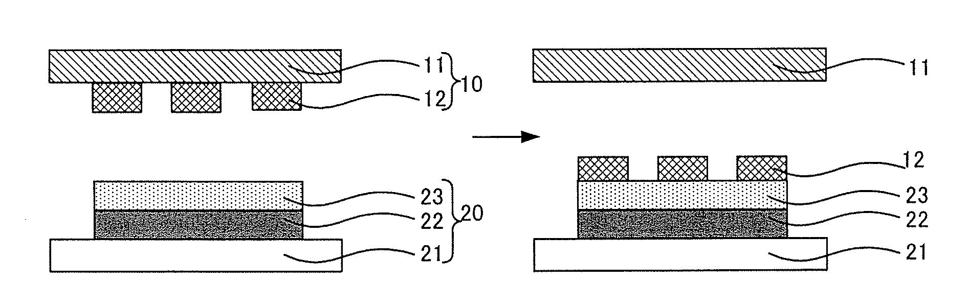
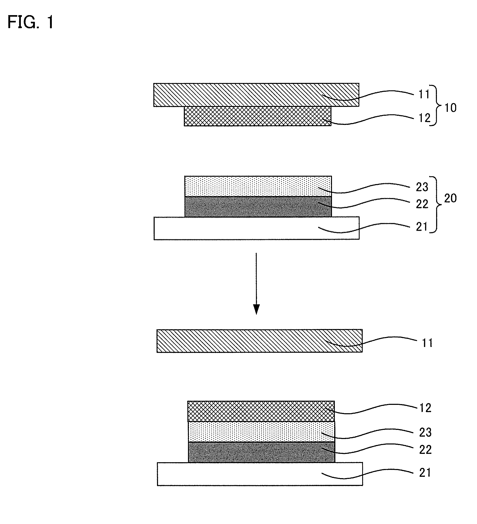
[0043]First, the first embodiment for manufacturing method of organic semiconductor device of the present invention will be explained. The manufacturing method of an organic semiconductor device of the present embodiment is to manufacture an organic semiconductor device having a technical structure where a bottom-gate type organic transistor is provided on a substrate.

[0044]In other words, the manufacturing method of an organic semiconductor device of the present embodiment comprises a step of transferring an organic semiconductor layer to a gate insulation layer by a thermal transfer at a liquid crystal phase transition temperature of a liquid crystalline organic semiconductor material, and the step uses: an organic semiconductor layer-transferring substrate comprising a parting substrate having parting properties, and the organic semiconductor layer formed on the parting substrate and containing the liquid...

second embodiment

B. Second Embodiment for Manufacturing Method of Organic Semiconductor Device

[0128]Next, the second embodiment of the manufacturing method of an organic semiconductor device of the present invention will be explained. The manufacturing method of an organic semiconductor device of the present embodiment is to manufacture an organic semiconductor device having a technical structure where a top-gate type organic transistor is provided on a substrate.

[0129]In other words, the manufacturing method of an organic semiconductor device of the present embodiment comprises a step of transferring an organic semiconductor layer to a substrate for forming an organic semiconductor device by a thermal transfer at a liquid crystal phase transition temperature of a liquid crystalline organic semiconductor material, and the step uses: an organic semiconductor layer-transferring substrate comprising a parting substrate having parting properties, and the organic semiconductor layer formed on the parting...

example 1

1. Example 1

(1) Liquid Crystal Phase Identification / Phase Transition Temperature Confirmatory Experiment

[0176]To confirm a liquid crystal phase and a phase transition temperature of a liquid crystalline organic semiconductor material 5,5′″-Dioctyl-2,2′:5′,2″:5″,2′″-Quaterthiophene (hereinafter, “8-QTP-8”), texture observation under a polarizing microscope (manufactured by Olympus Corporation, BH2-UMA®) using a heating stage (manufactured by Mettler-Toledo International Inc., FP82HT®, FP80HT®) and DSC (Differential Scanning calorimeter, manufactured by NETZSCH, DSC204 μ—Sensor®) measurement were carried out, and results of Iso 175.6, SmG 80.6 Cryst. (° C.) were obtained.

(2) Manufacture of Organic Semiconductor Layer-Transferring Substrate

[0177]A solution of 0.4 wt % TefonAF® (manufactured by Du Pont Kabushiki Kaisha) FC-40 Fluorinert® (manufactured by Sumitomo 3M Limited) was coated on a PEN substrate of 0.125 mm thickness by a spin coating (500 rpm, 10 seconds→1000 rpm, 20 seconds) ...


PUM


Abstract

The present invention provides a manufacturing method of an organic semiconductor device comprising a step of transferring an organic semiconductor layer to a gate insulation layer by a thermal transfer at a liquid crystal phase transition temperature of a liquid crystalline organic semiconductor material, and the step uses: an organic semiconductor layer-transferring substrate comprising a parting substrate having parting properties, and the organic semiconductor layer formed on the parting substrate and containing the liquid crystalline organic semiconductor material; and a substrate for forming an organic semiconductor device comprising a substrate, a gate electrode formed on the substrate, and the gate insulation layer formed to cover the gate electrode and having alignment properties which are capable of aligning the liquid crystalline organic semiconductor material on a surface of the gate insulation layer.

Description

TECHNICAL FIELD[0001]The present invention relates to a manufacturing method of an organic semiconductor device having a technical structure where an organic transistor is formed on a substrate.BACKGROUND ART[0002]The semiconductor transistor typified by TFT shows the current trend towards spreading of its applications along with the development of display devices. Such a semiconductor transistor functions as a switching element when the electrodes are connected through a semiconductor material.[0003]Here, as shown in FIGS. 13A and 13B, a transistor 100 using the semiconductor material normally comprises: a gate electrode 101, a gate insulation layer 102 for insulating the gate electrode 101, a semiconductor layer 103 made of the semiconductor material, a source electrode 104 and a drain electrode 105 formed so as to contact to the semiconductor layer 103. As such transistor, a transistor having a bottom-gate structure where the gate electrode 101 is provided to the under surface si...

Claims


Application Information

Patent Timeline
Patent Type & Authority Patents(United States)
IPC IPC(8): H01L51/40
CPCH01L51/0013H01L51/003H01L51/0076H01L51/0545H01L51/0558H10K71/18H10K71/80H10K85/731H10K10/484H10K10/466
Inventor TOMINO, KENMATSUOKA, MASANAOSUZUKI, TOMOMIMAEDA, HIROKI
Owner DAI NIPPON PRINTING CO LTD
Why Eureka
Try Eureka