Bipolar transistor with diffused layer between deep trench sidewall and collector diffused layer

a bipolar transistor and collector technology, applied in the field of bipolar transistors, can solve the problems of low gm (mutual conductance) compared to a bipolar transistor, deterioration of flicker noise characteristics (also referred to as 1/f noise characteristics), and low gm (mutual conductance) of mos transistors, so as to improve transistor characteristics, excellent transistor characteristics, and reduce leakage current

Inactive Publication Date: 2014-04-29
PANASONIC CORP
View PDF19 Cites 2 Cited by
  • Summary
  • Abstract
  • Description
  • Claims
  • Application Information

AI Technical Summary

Benefits of technology

[0046]According to the semiconductor device in the present invention, transistor characteristics can be improved because a leakage current can be reduced.
[0047]Moreover, according to the method of manufacturing the semiconductor device in the present invention, a semiconductor device having excellent transistor characteristics can be manufactured with a small number of processes.

Problems solved by technology

However, a MOS transistor has a drawback in that gm (mutual conductance) is low compared to a bipolar transistor.
Moreover, in the case where the MOS transistor is used, the current flowing between the source and the drain flows on the surface of a semiconductor substrate and is, therefore, easily influenced by a crystal lattice defect which exists on the surface of the semiconductor substrate.
As a result, in this case, flicker noise characteristics (also referred to as 1 / f noise characteristics) deteriorate compared to the case where the bipolar transistor is used.
Moreover, in comparison between mismatch characteristics (the difference in threshold voltages in a pair transistor) which are important in the analog circuit, the characteristics of the MOS transistor are inferior to the characteristics of the bipolar transistor.
If the bipolar transistor is to be embedded in the digital circuit, a bipolar transistor process becomes necessary in addition to the CMOS process, which causes problems such as increased cost due to an increase in the number of steps for the process, and deterioration of the characteristics of the MOS transistor due to the addition of thermal treatment and processes for forming the bipolar transistor.
Moreover, since the area of the bipolar transistor is larger than that of the MOS transistor, there is a problem of an increase in cost due to an increase in the area of a chip.

Method used


Image

  • Bipolar transistor with diffused layer between deep trench sidewall and collector diffused layer
  • Bipolar transistor with diffused layer between deep trench sidewall and collector diffused layer
  • Bipolar transistor with diffused layer between deep trench sidewall and collector diffused layer

Examples


embodiment 1

[0064]The following describes a semiconductor device and a method of manufacturing the same according to an embodiment of the present invention with reference to the drawings. It is to be noted that the diagrams are schematic diagrams, and the illustration is not necessarily strictly accurate.

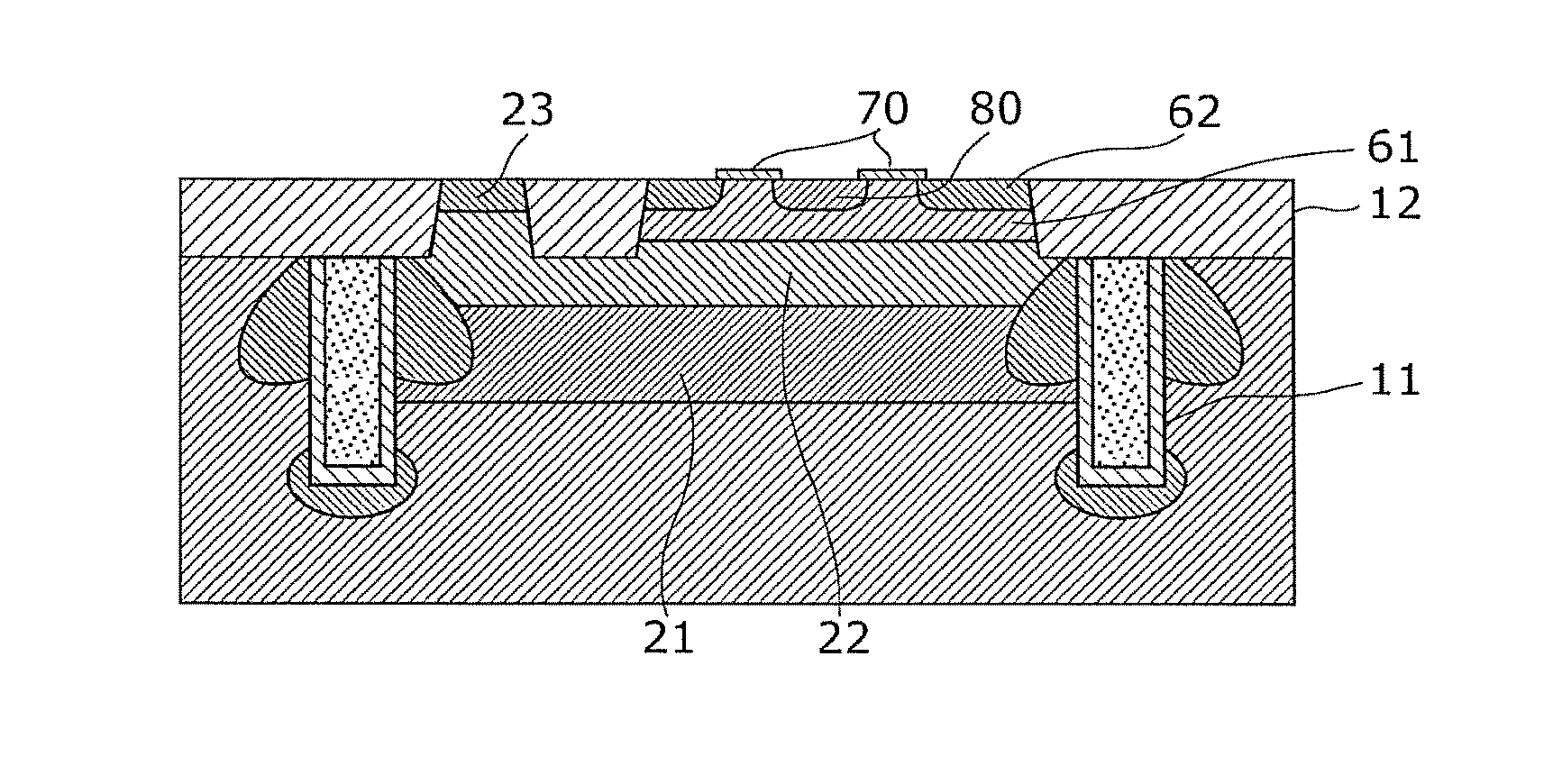
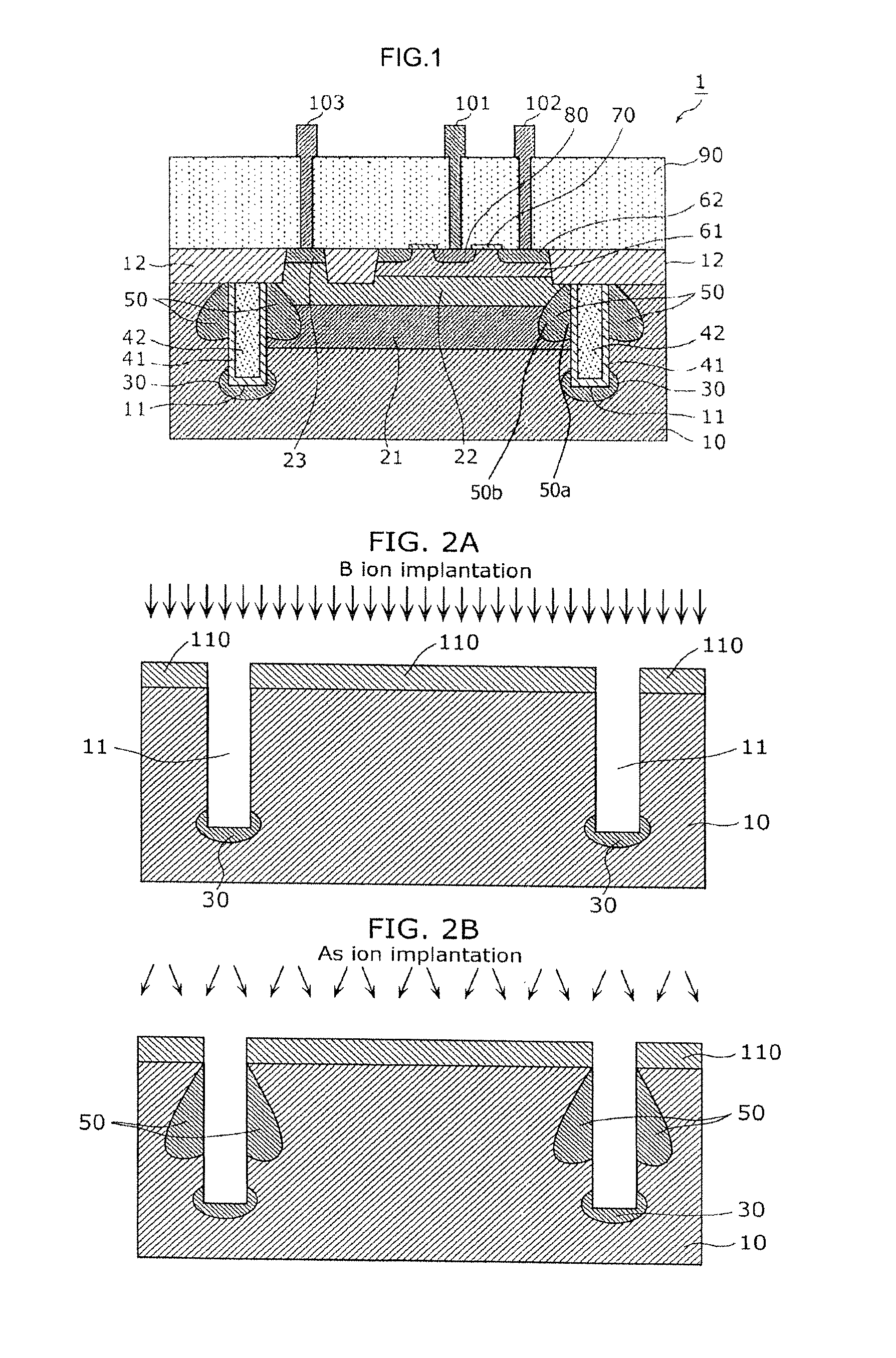
[0065]The following describes a semiconductor device 1 according to the embodiment of the present invention with reference to FIG. 1. FIG. 1 is a cross-sectional view showing a structure of the semiconductor device according to the embodiment of the present invention.

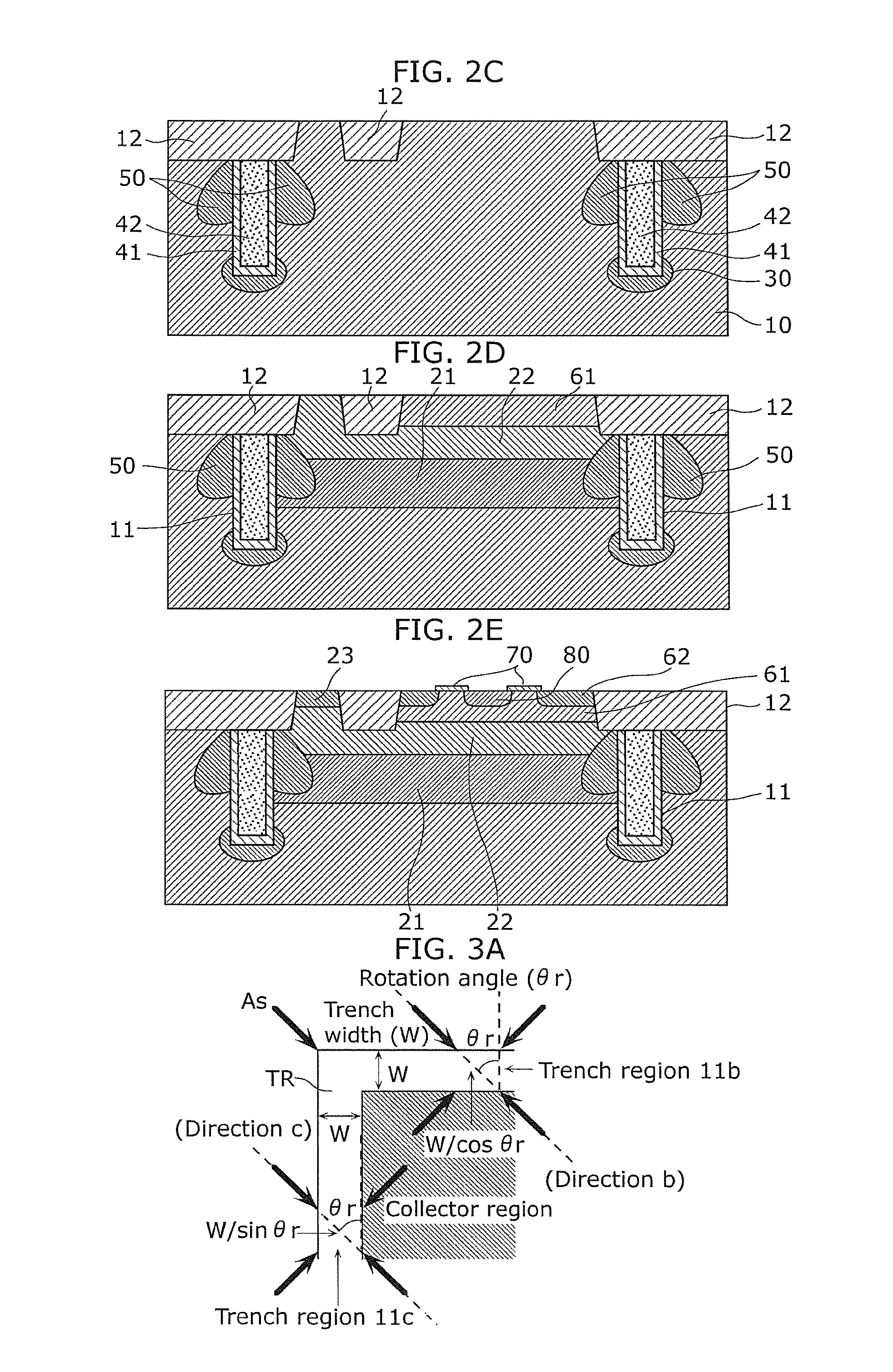
[0066]The semiconductor device 1 according to the embodiment of the present invention is, as shown in FIG. 1, a vertical NPN bipolar transistor in which an isolation trench including a deep trench (Deep Trench Isolation: DTI) 11 that is a first trench and a shallow trench (Shallow Trench Isolation: STI) 12 that is a second trench is formed as an isolation region for isolating the bipolar transistor from other devices and the like i...


PUM


Abstract

A semiconductor device according to the present invention includes a p-type semiconductor substrate, a first n-type collector diffusion layer formed in the p-type semiconductor substrate, a deep trench formed in the p-type semiconductor substrate so as to surround the first n-type collector diffusion layer, a p-type channel stopper layer formed beneath the deep trench, and an n-type diffusion layer formed between a sidewall of the deep trench and the first n-type collector diffusion layer.

Description

CROSS REFERENCE TO RELATED APPLICATIONS[0001]This is a continuation application of PCT Patent Application No. PCT / JP2011 / 003560 filed on Jun. 22, 2011, designating the United States of America, which is based on and claims priority of Japanese Patent Application No. 2010-164368 filed on Jul. 21, 2010. The entire disclosures of the above-identified applications, including the specifications, drawings and claims are incorporated herein by reference in their entirety.TECHNICAL FIELD[0002]The present invention relates to semiconductor devices and methods of manufacturing the same, and particularly to a high-performance and low-cost bipolar transistor used in a semiconductor integrated circuit and a method of manufacturing the same.BACKGROUND ART[0003]In recent years, along with increased integration and increased functionality of semiconductor integrated circuits, enhancement in performance of analog-digital mixed-signal integration circuits on which analog signal processing circuits (a...

Claims


Application Information

Patent Timeline
Patent Type & Authority Patents(United States)
IPC IPC(8): H01L29/735
CPCH01L29/735H01L29/0821H01L29/66272H01L21/76237H01L29/045H01L29/7322
Inventor TANAKA, MITSUOSANO, TSUNEICHIROMATSUI, OSAMU
Owner PANASONIC CORP
Why Eureka
Try Eureka