


Quick Research
Generate reliable direction feasibility study reports for your R&D in just a few steps.

Technical Q&A
Discover and master advanced knowledge NOW. Basics, ideas, possibilities, all at once.

Find Solutions
As an expert in R&D theories, this can generate solutions to your technical problems instantly.

Evaluate Feasibility
Analyze your overall solution with one click, know your potential R&D risks in advance.

Monitor Landscape
Get weekly tech updates, stay abreast of the latest tech innovations and key insights.
Micromechanical pressure sensor device and corresponding manufacturing method
- Summary
- Abstract
- Description
- Claims
- Application Information
AI Technical Summary
Benefits of technology
Problems solved by technology
Method used
Image

Examples
Embodiment Construction
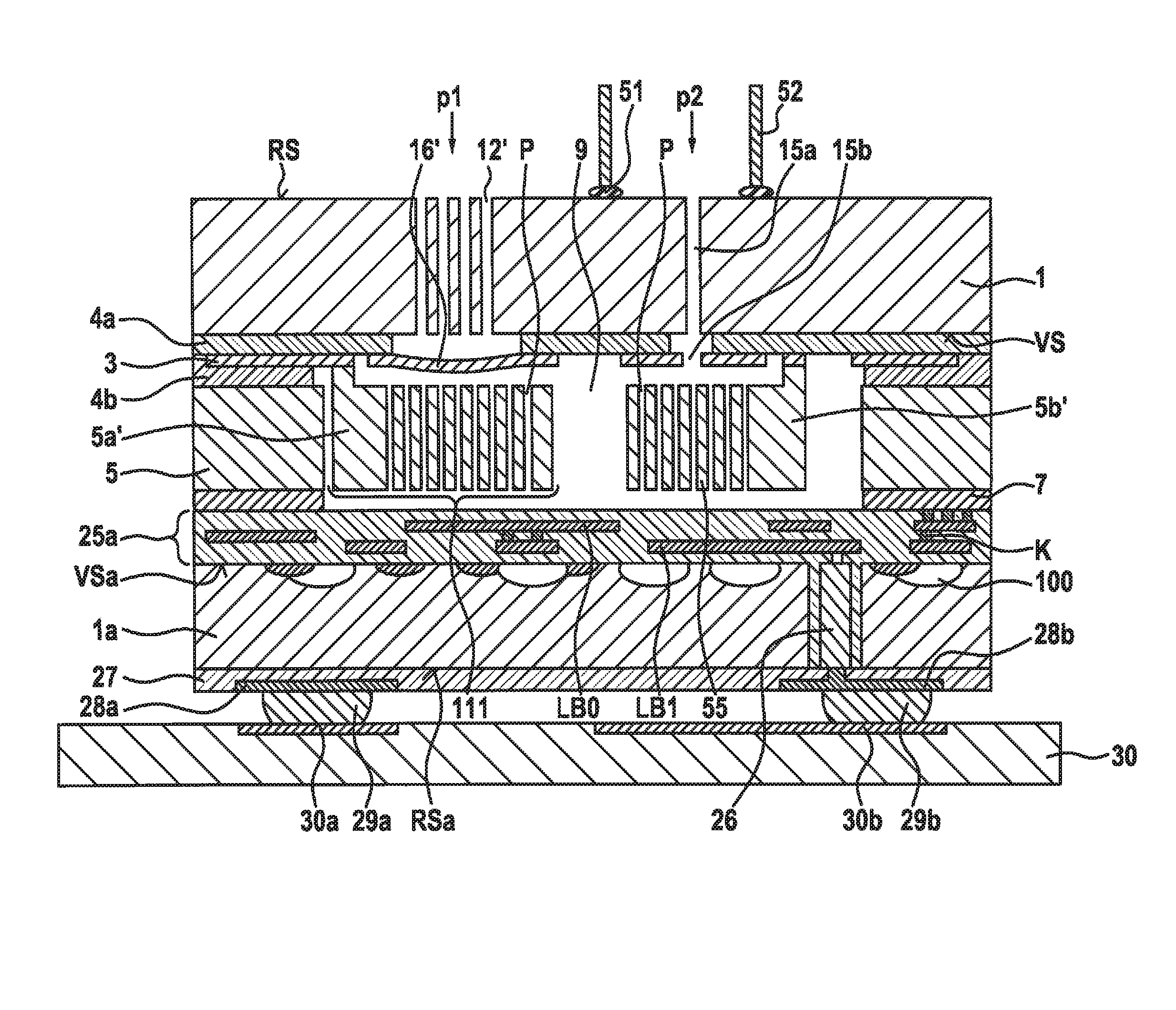
[0036]Identical or functionally equivalent elements are denoted by the same reference numerals in the figures.
[0037]FIG. 1 is a schematic cross-sectional view for explaining an exemplary micromechanical pressure sensor device and a corresponding manufacturing method.
[0038]In FIG. 1, reference numeral 1 denotes an ASIC wafer which includes a plurality of CMOS circuits 100 which include, for example, an evaluation circuit for the micromechanical pressure sensor device to be formed.
[0039]ASIC wafer 1a has a front side VSa and a rear side RSa. On front side VS of ASIC wafer 1, a rewiring system 25a is formed which includes a plurality of strip conductor levels LB0, LB1 and insulating layers I situated in between. To simplify the illustration, insulating layers I in which strip conductor levels LB0, LB1 are embedded are not separately illustrated. The strip conductor sections of strip conductor levels LB0, LB1 are electrically connected to one another by electrically conductive vias K.
[0...
PUM
 Abstract
Description
Claims
Application Information
 - R&D Engineer
- R&D Manager
- IP Professional
- Industry Leading Data Capabilities
- Powerful AI technology
- Patent DNA Extraction
Browse by: Latest US Patents, China's latest patents, Technical Efficacy Thesaurus, Application Domain, Technology Topic, Popular Technical Reports.
© 2024 PatSnap. All rights reserved.Legal|Privacy policy|Modern Slavery Act Transparency Statement|Sitemap|About US| Contact US: help@patsnap.com