Semiconductor assembly

Active Publication Date: 2016-11-10
HITACHI ENERGY SWITZERLAND AG
View PDF7 Cites 7 Cited by
  • Summary
  • Abstract
  • Description
  • Claims
  • Application Information

AI Technical Summary

Benefits of technology

[0005]An object of the present invention is to provide

Problems solved by technology

This means that a large number of heavy and sometime expe

Method used


Image

  • Semiconductor assembly
  • Semiconductor assembly
  • Semiconductor assembly

Examples


second embodiment

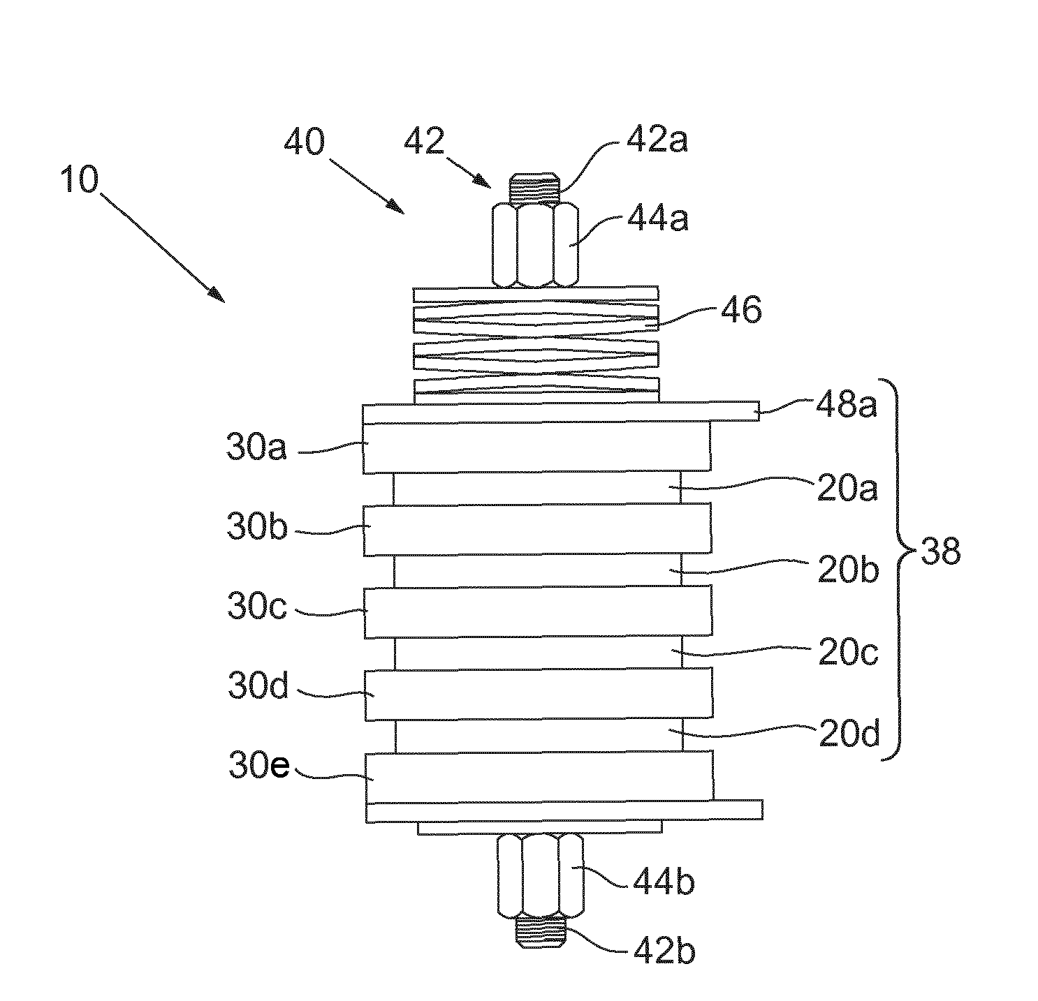
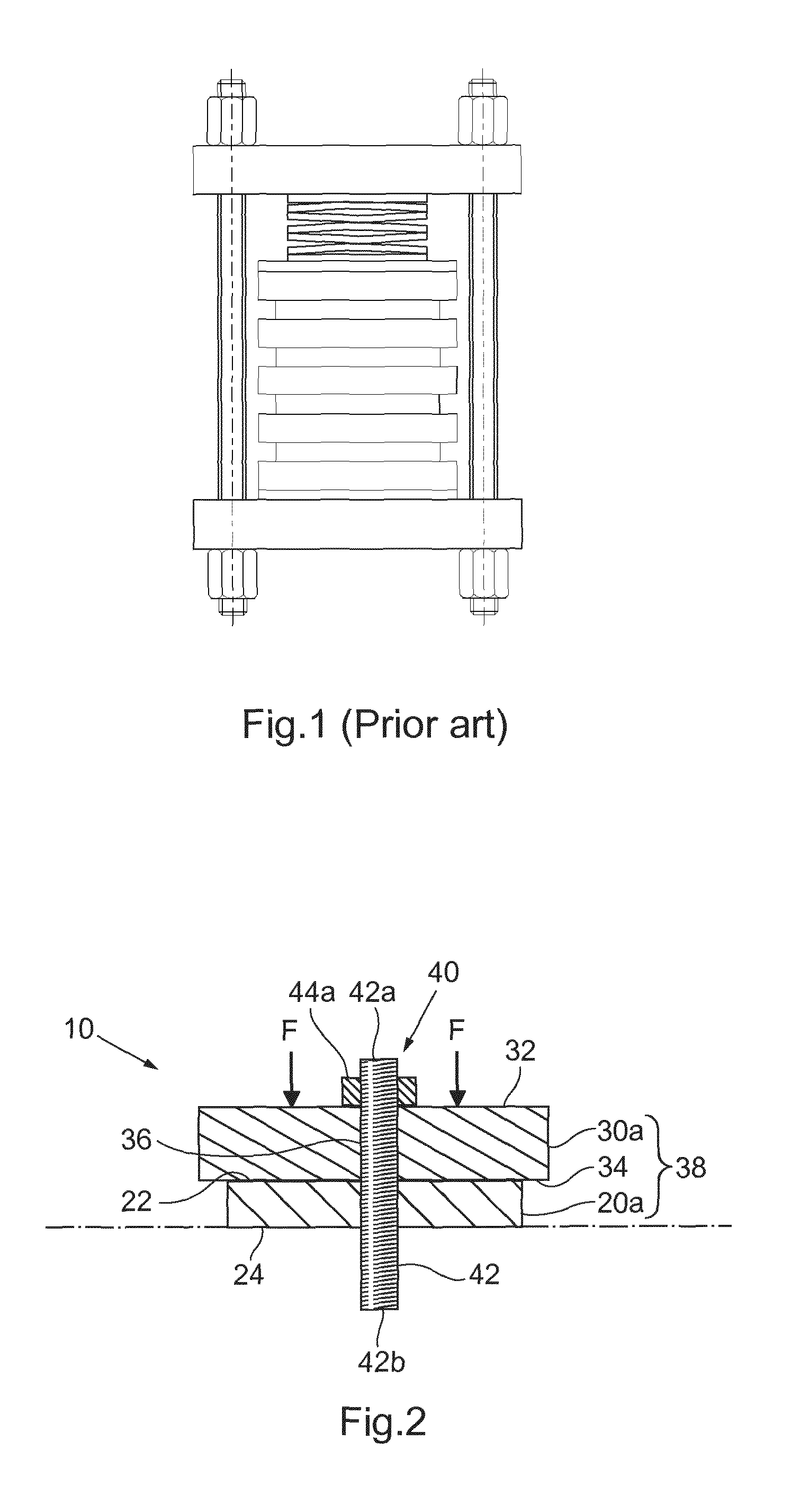
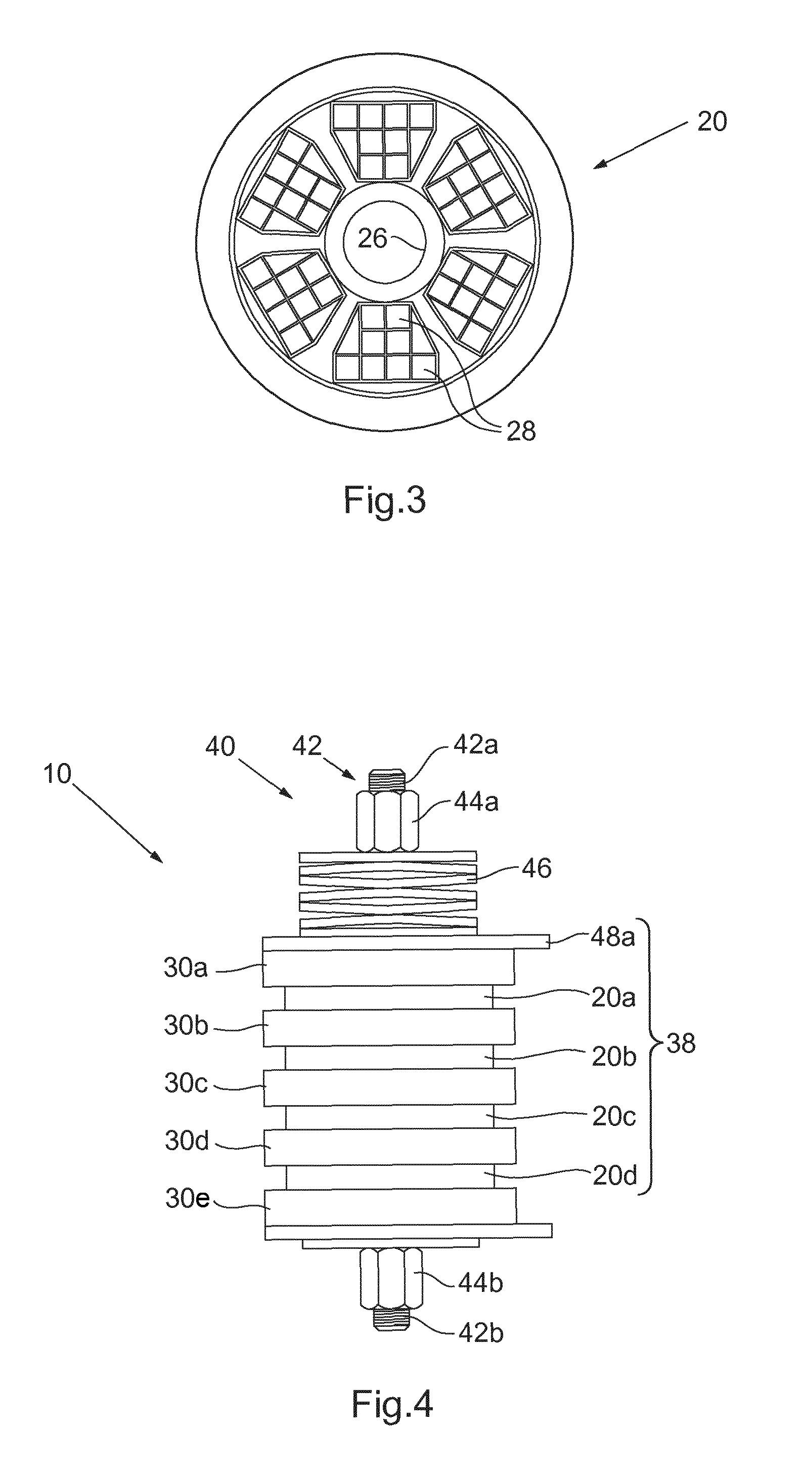
[0034]a semiconductor assembly will now be described with reference to FIG. 4. In this embodiment, a plurality, namely four semiconductor modules 20a, 20b, 20c, 20d, are provided in a stack. Correspondingly, a plurality of coolers, namely five coolers 30a, 30b, 30c, 30d, 30e, are provided in such a way that each of the semiconductor modules 20a-d is provided between two of the coolers 30a-e. This means that the semiconductor modules 20a-d and the coolers 30a-e are arranged alternately in a stack 38 having a first upper end as shown in the figure and a second, opposite lower end.

[0035]A clamping assembly 40 comprises a bar 42 with a first upper threaded end portion 42a and a second lower threaded end portion 42b. A first clamping element in the form of a first nut 44a is threaded onto the first end portion 42a of the bar and a second clamping element in the form of a second nut 44b is threaded onto the second end portion 42b of the bar.

[0036]A spring package 46 is arranged between th...

third embodiment

[0040]a semiconductor assembly will now be described with reference to FIG. 5. In this embodiment, a plurality, namely two semiconductor modules 20a, 20b, are provided in a stack 38. Correspondingly, a plurality of coolers, namely three coolers 30a, 30b, 30c, are provided in such a way, that each of the semiconductor modules 20a, 20b is provided between two of the coolers 30a-c. This means that also in this embodiment the semiconductor modules 20a, 20b, and the coolers 30a-c are arranged alternately in a stack 38 having a first upper end as shown in the figure and a second, opposite lower end.

[0041]A clamping assembly 40 comprises a bar 42 with an upper threaded end portion 42a. The lower end portion 42b of the bar 42 is attached to a piece of electrical equipment, such as a capacitor. A clamping element in the form of a nut 44a is threaded onto the upper end portion 42a of the bar.

[0042]A spring package 46, similar to the one shown in FIG. 4, is arranged between the first nut 44a a...

fourth embodiment

[0047]a semiconductor assembly will now be described with reference to FIGS. 6-8. In this embodiment, a plurality, namely two semiconductor modules 20a, 20b are provided in a stack 38. Correspondingly, a plurality of coolers, namely three coolers 30a, 30b, 30c are provided in such a way, that each of the semiconductor modules 20a, 20b is provided between two of the coolers 30a-c. This means that also in this embodiment the semiconductor modules 20a, 20b and the coolers 30a-c are arranged alternately in a stack 38 having a first upper end as shown in the figure and a second, opposite lower end.

[0048]A clamping assembly 40 comprises a bar 42 with an upper threaded end portion 42a. A clamping element in the form of a nut 44a is threaded onto the upper end portion 42a of the bar 42, acting as a bus bar. The lower end portion 42b of the bar 42 is attached to a piece of electrical equipment in the form of a capacitor 60, preferably by means of a screw joint, wherein the capacitor is provi...


PUM


Abstract

A semiconductor assembly includes a stack with a semiconductor module and a cooler, wherein the semiconductor module is provided in contact with the cooler. A clamping assembly is adapted to exert a force on the two sides of the stack. The stack is provided with a through hole between the two sides thereof and a part of the clamping assembly including an electrically conductive part which extends through the through hole of the stack. Thereby, a compact mechanical arrangement is provided while obtaining improved electrical properties, such as lower inductance and more even current distribution.

Description

TECHNICAL FIELD[0001]The present invention relates generally to semiconductor assemblies and more particularly to a semiconductor assembly comprising a press pack module.BACKGROUND ART[0002]Many different types of electrical converters make use of press pack modules for their easiness to bring them into series connection with the help of a mechanical stack, where more than one module is provided in series. Press pack modules are made to be mounted in between cooler or pressure plates and pressure is applied to that stack to ensure proper electrical and thermal contact between the individual press pack modules. For HVDC converters, up to 20 modules can be put in series connection into one stack and more than a hundred stacks can be needed for the complete converter. This means that a large number of heavy and sometime expensive mechanical parts are needed to create those stacks.[0003]An example of a prior art press pack stack is disclosed in FIG. 1. As seen in this figure, a standard...

Claims


Application Information

Patent Timeline
IPC IPC(8): H01L23/40H02M7/00H01L25/07H01L25/11H01L23/367H01L23/473
CPCH01L23/4012H01L23/3675H01L23/473H01L25/074H01L2023/4081H02M7/003H01L2023/4087H01L2023/4031H01L25/117H01L23/4006H01L25/071H01L25/16H05K7/209H01L24/72H01L2924/1305H01L2924/13055H01L2924/00
Inventor EKWALL, OLLEDORE, ERIKDUGAL, FRANCSCHNELL, RAFFAEL
Owner HITACHI ENERGY SWITZERLAND AG
Why Eureka
Try Eureka