Encapsulated semiconductor device and encapsulation method

a technology of encapsulation and semiconductor, applied in semiconductor devices, solid-state devices, organic semiconductor devices, etc., can solve the problems of reducing the service life of the substrate. , to achieve the effect of reducing side leakag

Inactive Publication Date: 2016-11-24
OLEDWORKS GMBH
View PDF0 Cites 15 Cited by
  • Summary
  • Abstract
  • Description
  • Claims
  • Application Information

AI Technical Summary

Benefits of technology

[0007]It is an object of the present invention to provide an encapsulated semiconductor device on a flexible substrate, in particular an encapsulated organic light emitting diode device on a flexible substrate overcoming the above drawbacks in the context of large area substrates or roll-to-roll processes. It is a further object of the present invention to provide for a method of at least partially encapsulating a semiconductor device like an organic light emitting diode device on a flexible substrate. The present invention aims at providing cuttable OLEDs, for example, to be cut out of a larger flexible substrate or in the context of a roll-to-roll process while reducing side leakage. Other encapsulated semiconductor devices, in particular photovoltaic and organic photovoltaic devices, are also foreseen.

Problems solved by technology

However, a disadvantage of using current plastics lies in that today's flexible plastic substrates do not provide a sufficient moisture barrier and therefore an (additional) encapsulation from the substrate side is needed.
When an OLED, for example, provided on top of such TFE barrier layer on a flexible substrate is cut out of large area plastic substrates or out of the roll that is being used in a roll-to-roll process, the substrate encapsulation is damaged and a leakage path is opened up.
In other words, upon cutting through OLEDs on a plastic foil substrate, the TFE barrier layer on the substrate side is damaged, and thus, from the sides, moisture can enter the organic layer.
If the moisture reaches, through a pinhole in the inner inorganic layer or the like, the OLED, the access results in a black spot, which will furthermore grow with time.

Method used


Image

  • Encapsulated semiconductor device and encapsulation method
  • Encapsulated semiconductor device and encapsulation method
  • Encapsulated semiconductor device and encapsulation method

Examples


Embodiment Construction

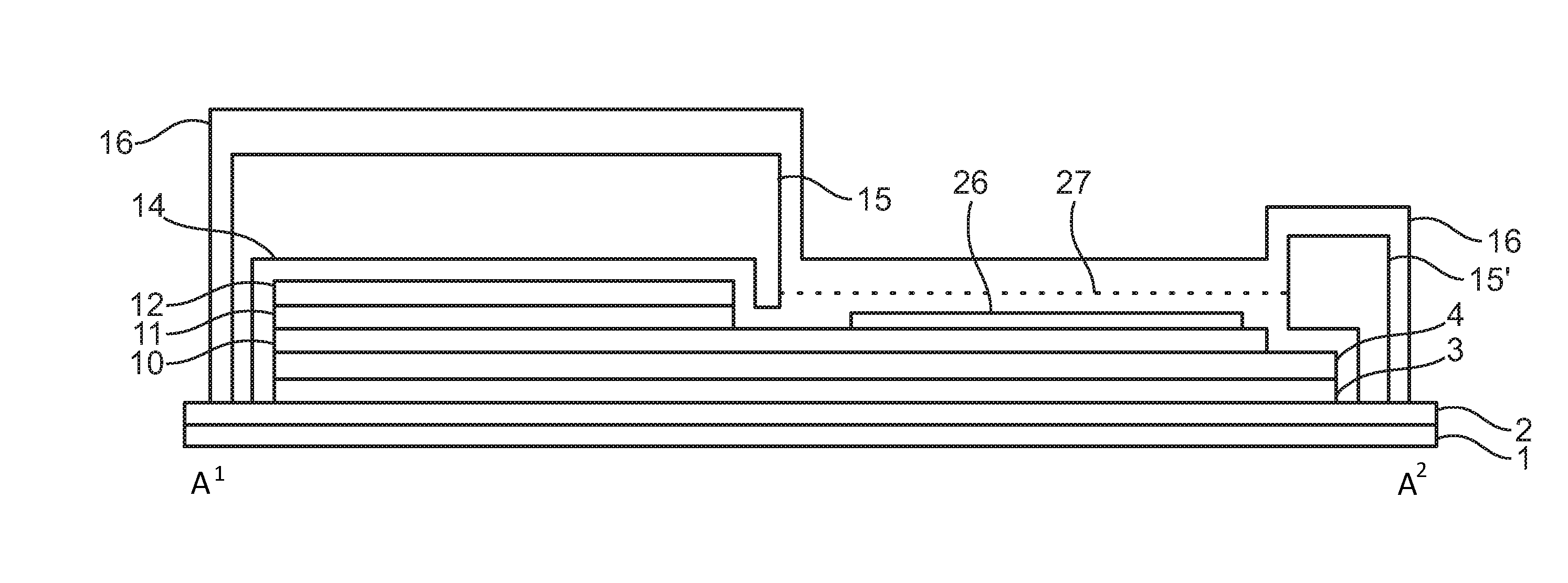
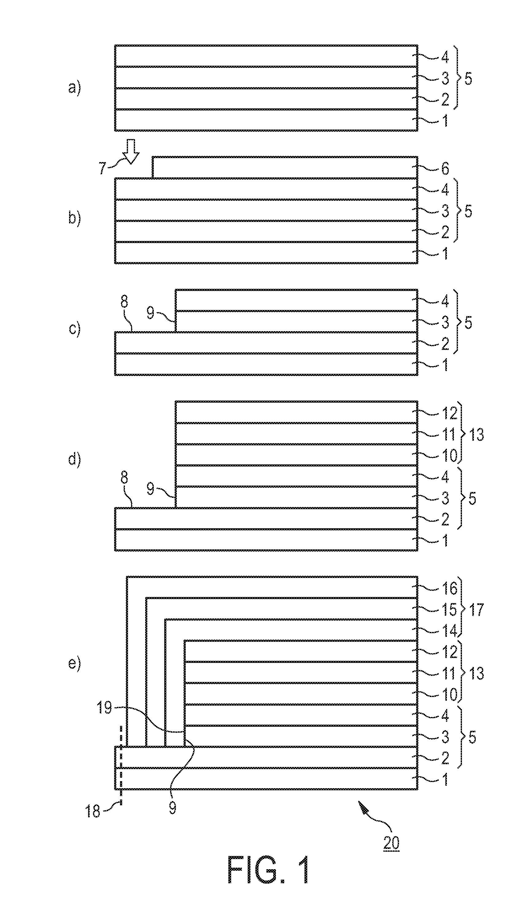
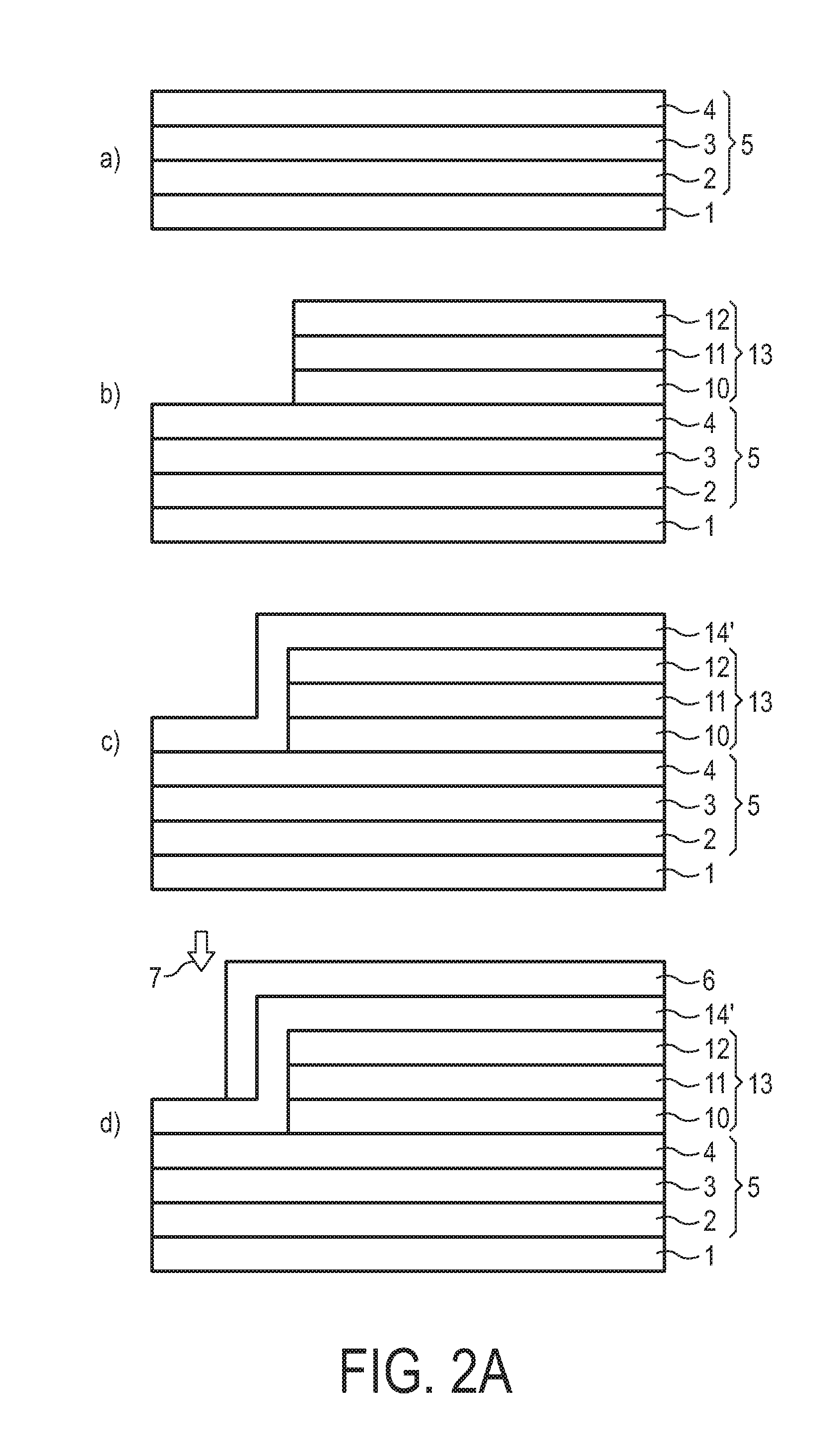
[0047]FIG. 1 illustrates a first concept for providing an encapsulated OLED device in accordance with an embodiment of the invention.

[0048]A barrier layer 5 is provided on a plastic foil 1 as a substrate. The barrier layer 5 includes an outer inorganic barrier layer 2 made of SiN, an organic barrier layer 3 and an inner inorganic barrier layer 4 (also made of SiN), as shown in FIG. 1a).

[0049]FIG. 1b) shows an organic etch mask 6 printed on top of the barrier 5 on a pre-defined area. In this case, the area left free by the etch mask 6 is at an edge of the plastic foil 1. As indicated by arrow 7, a SiN plasma etch process is applied to remove a part of the upper SiN layer (the inner inorganic layer 4) at the non-covered area. After that a second organic plasma etch process (not shown) is applied which removes a part of the organic barrier layer 3 of the barrier stack 5 and the organic etch mask 6 at the same time. After plasma etching the organic barrier layer 3 is fully removed from ...


PUM


Abstract

The present invention relates to an encapsulated semiconductor device (20) provided on a flexible substrate (1), a method of providing an at least partially encapsulated semiconductor device (20) on a flexible substrate (1) and a software product for providing an at least partially encapsulated semiconductor device (20) on a flexible substrate (1). In a preferred embodiment, an encapsulation method is presented in which the organic layer (3) of an inorganic/organic/inorganic multilayer barrier (5) on a plastic foil (1) as a substrate is removed at the edges of an OLED (13). The edges are subsequently sealed with a standard TFE process to encapsulate the OLED (13). This enables cuttable OLEDs (20) that are cut out of a larger plastic substrate (1) and gives a method to reduce side leakage in OLEDs (20) that have been manufactured in a roll-to-toll process.

Description

FIELD OF THE INVENTION[0001]The present invention relates to an encapsulated semiconductor device on a flexible substrate, in particular an encapsulated organic light emitting diode device provided on a flexible substrate, and to a method of providing an at least partially encapsulated semiconductor device like an organic light emitting diode device on a flexible substrate.BACKGROUND OF THE INVENTION[0002]Organic light emitting diode devices (in the following referred to as OLED device or simply OLED) can be made on flexible substrates. One prominent option is to use plastic substrates. Similarly, also other semiconductor devices (in particular organic semiconductor devices) can be provided on flexible substrates. Particular examples are photovoltaic devices and particularly organic photovoltaic devices (OPV).[0003]An advantage of using plastic substrates lies in the possibility of using transparent plastics.[0004]However, a disadvantage of using current plastics lies in that today'...

Claims


Application Information

Patent Timeline
Patent Type & Authority Applications(United States)
IPC IPC(8): H01L51/52H01L51/44H01L51/00
CPCH01L51/5256H01L51/0097H01L2251/566H01L2251/5338H01L51/448Y02E10/549H10K50/8445H10K71/851H10K2102/311H10K30/88H10K77/111
Inventor MEYER, JENSGIERTH, RAINALD MANFREDGRABOWSKI, STEFAN PETERLIFKA, HERBERTVAN DE WEIJER, PETERBOUTEN, PETRUS CORNELIS-PAULUSVAN ELSBERGEN, VOLKER LAMBERTRUSKE, MANFRED STEPHANHARTMANN, SOREN
Owner OLEDWORKS GMBH
Why Eureka
Try Eureka