Organic light emitting diode display

a light-emitting diode and organic technology, applied in the field of organic light-emitting diodes (oled) displays, can solve the problems of low luminance or low luminous efficiency, relatively high driving voltage, and limited response speed and viewing angle, so as to increase the luminous efficiency of the oled display and reduce the interfacial resistance of the electrod

Active Publication Date: 2016-12-01
SAMSUNG DISPLAY CO LTD
View PDF0 Cites 8 Cited by
  • Summary
  • Abstract
  • Description
  • Claims
  • Application Information

AI Technical Summary

Benefits of technology

[0027]As previously discussed, according to some example embodiments of the present invention, the intermediate layer including an ionic conductor material may be formed between the electrode and the emission layer to reduce the interfacial resistance of the electrode and to uniformly form the surface, thereby increasing luminous efficiency of the OLED display.

Problems solved by technology

However, because LCDs are passive light-emitting devices, they may utilize separate backlights and may have limitations in terms of response speed and viewing angle.
However, related art OLED displays have problems in that they may require a relatively high driving voltage, may have relatively low luminance or low luminous efficiency, and may have a short light-emitting service life.

Method used


Image

  • Organic light emitting diode display
  • Organic light emitting diode display
  • Organic light emitting diode display

Examples


Embodiment Construction

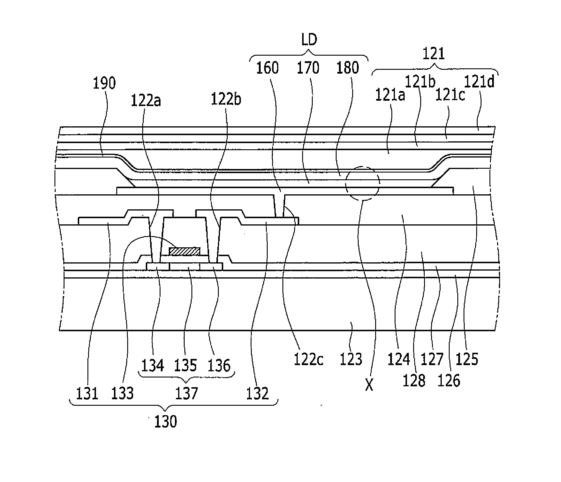
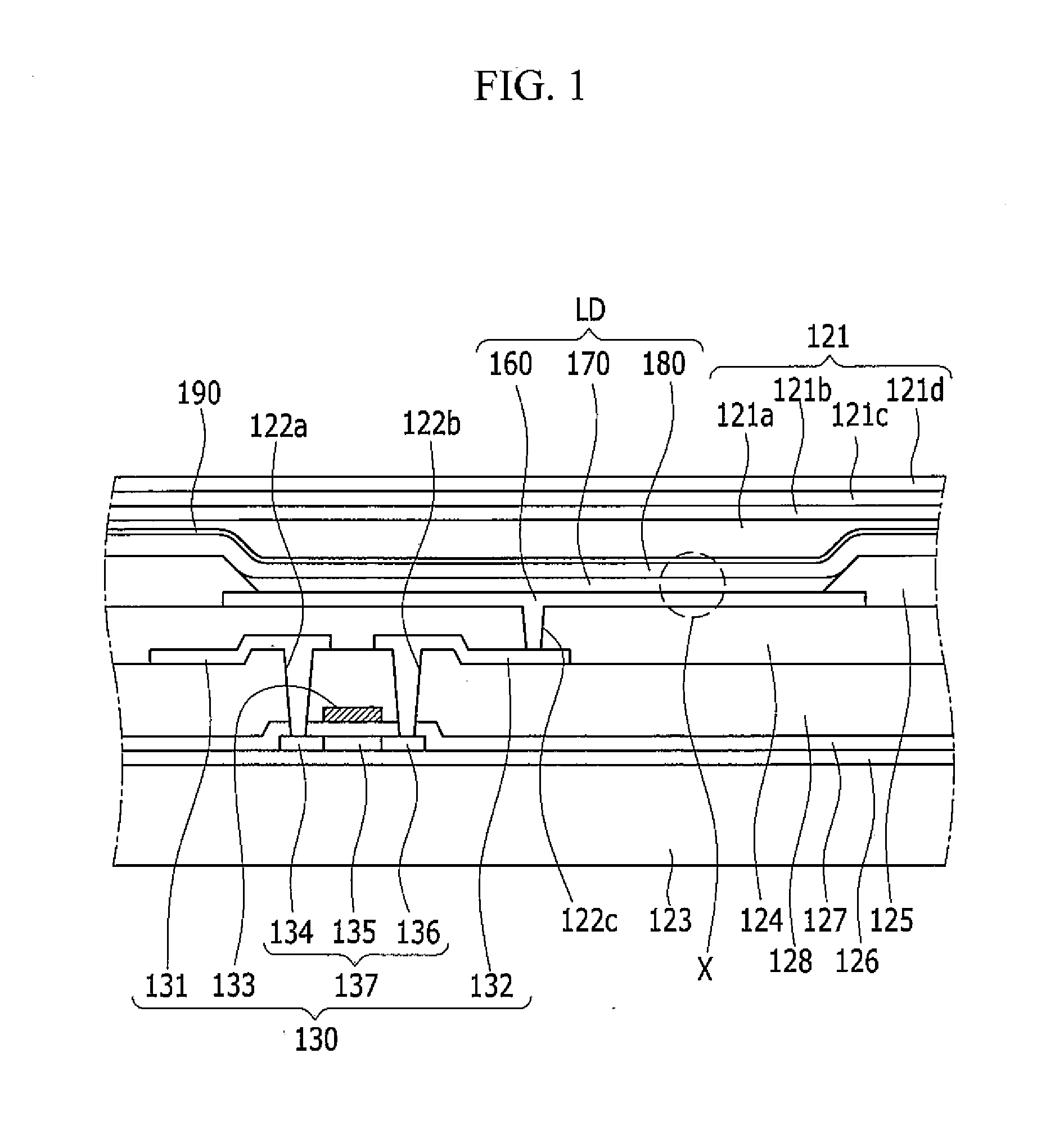
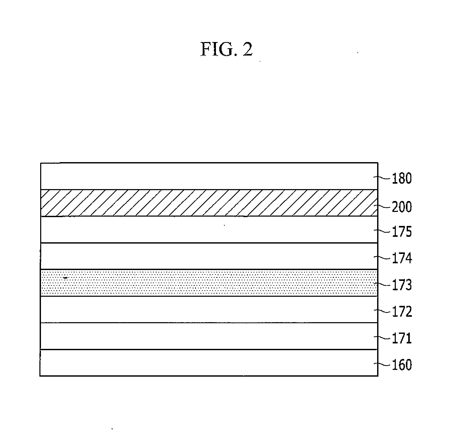
[0032]Aspects of example embodiments of the present invention will be described more fully hereinafter with reference to the accompanying drawings, in which example embodiments of the present invention are shown. As those skilled in the art would realize, the described embodiments may be modified in various different ways, all without departing from the spirit or scope of the present invention.

[0033]It will be understood that, although the terms “first,”“second,”“third,” etc., may be used herein to describe various elements, components, regions, layers and / or sections, these elements, components, regions, layers and / or sections should not be limited by these terms. These terms are used to distinguish one element, component, region, layer or section from another element, component, region, layer or section. Thus, a first element, component, region, layer or section described below could be termed a second element, component, region, layer or section, without departing from the spirit...


PUM


Abstract

An organic light emitting diode (OLED) display includes: a thin film transistor on the substrate; a first electrode electrically connected to the thin film transistor; a hole injection layer on the first electrode; an emission layer on the hole injection layer; an electron injection layer on the emission layer; a first intermediate layer on the electron injection layer; and a second electrode on the first intermediate layer.

Description

CROSS-REFERENCE TO RELATED APPLICATION[0001]This application claims priority to and the benefit of Korean Patent Application No. 10-2015-0074879 filed in the Korean Intellectual Property Office on May 28, 2015, the entire content of which is incorporated herein by reference.BACKGROUND[0002]1. Field[0003]Aspects of embodiments of the present invention relate to an organic light emitting diode (OLED) display.[0004]2. Description of the Related Art[0005]Recently, consumer demand for light and slim monitors or televisions has increased, and due to such demand, cathode ray tubes (CRTs) have been replaced by alternative technologies, such as liquid crystal displays (LCDs). However, because LCDs are passive light-emitting devices, they may utilize separate backlights and may have limitations in terms of response speed and viewing angle.[0006]Recently, organic light emitting diode (OLED) displays have been receiving great attention as display devices capable of overcoming such limitations, ...

Claims


Application Information

Patent Timeline
Patent Type & Authority Applications(United States)
IPC IPC(8): H01L51/52H01L51/50H01L27/32
CPCH01L51/5212H01L27/3248H01L51/5092H01L2251/301H01L51/5228H01L2251/558H01L51/5072H10K50/171H10K50/17H10K50/814H10K50/16H10K50/824H10K59/123H10K2102/00H10K2102/351
Inventor KIM, DONG CHANKIM, WON JONGHAN, WON SUKKIM, EUNG DOSEO, DONG KYULEEYIM, SANG HOON
Owner SAMSUNG DISPLAY CO LTD
Why Eureka
Try Eureka